Method for aging trench gate VDMOS device and aging equipment

A device aging and aging equipment technology, applied in the direction of single semiconductor device testing, instruments, measuring devices, etc., can solve the problems of rapid inspection of separated gate trench VDMOS devices, injection, lack of automatic monitoring and control, etc., to achieve fast and effective. The effect of aging assessment screening

CN111983416APending Publication Date: 2020-11-24无锡摩斯法特电子有限公司
10 Cites 0 Cited by

Patent Information

Authority / Receiving Office
CN · China
Patent Type
Applications(China)
Current Assignee / Owner
Publication Date
2020-11-24

Smart Images

  • Figure 1
    Figure 1
  • Figure 2
    Figure 2
  • Figure 3
    Figure 3
Patent Text Reader

Abstract

The embodiment of the invention relates to a method for aging a trench gate VDMOS device and aging equipment. The method comprises the following steps: enabling a control circuit to output a first control signal, and controlling a controllable voltage source to apply a positive voltage to a drain electrode of a to-be-aged VDMOS device till the positive voltage reaches a breakdown voltage of the to-be-aged VDMOS device; within the set aging time, enabling the control circuit to acquire a first real-time monitoring signal of the drain-source current of the to-be-aged VDMOS device, acquiring a second real-time monitoring signal of the device surface temperature of the to-be-aged VDMOS device, and outputting a second control signal according to the first real-time monitoring signal and the second real-time monitoring signal; enabling the controllable voltage source to adjust the output voltage according to the second control signal to enable the drain-source current of the to-be-aged VDMOSdevice to be within a first preset range and the surface temperature of the device to be within a second preset range; and after timing is finished, cooling the to-be-aged VDMOS device, and taking out the to-be-aged VDMOS device from the aging equipment to obtain the aged trench gate VDMOS device.
Need to check novelty before this filing date? Find Prior Art

Description

technical field

[0001] The invention relates to the technical field of semiconductor devices, in particular to a aging method and aging equipment for trench gate VDMOS devices. Background technique

[0002] Before power devices are put into mass production and during the mass production process, in order to ensure that the life of the devices under working conditions can meet our requirements, an accelerated life simulation aging assessment of high temperature and high pressure will be arranged. At present, the reliability aging of vertical conductive double-diffused structure field effect transistors (VDMOS) includes high temperature drain-source voltage reverse bias (High temperature reverse bias, HTRB) and high temperature gate-source voltage reverse bias (High temperature gate bias, HTGB), where HTGB It is to carry out the aging assessment on the gate oxide between the gate and the source, because its voltage is low, generally not exceeding 20V. The HTRB assessment is g...

Examples

Embodiment Construction

[0020] The technical solutions of the present invention will be described in further detail below with reference to the accompanying drawings and embodiments.

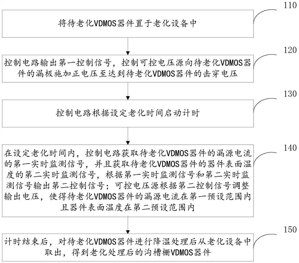
[0021] An embodiment of the present invention provides a method for aging a trench gate VDMOS device, the process of which is as follows figure 1 As shown, it mainly includes the following steps:

[0022] Step 110, placing the VDMOS device to be aged in an aging device;

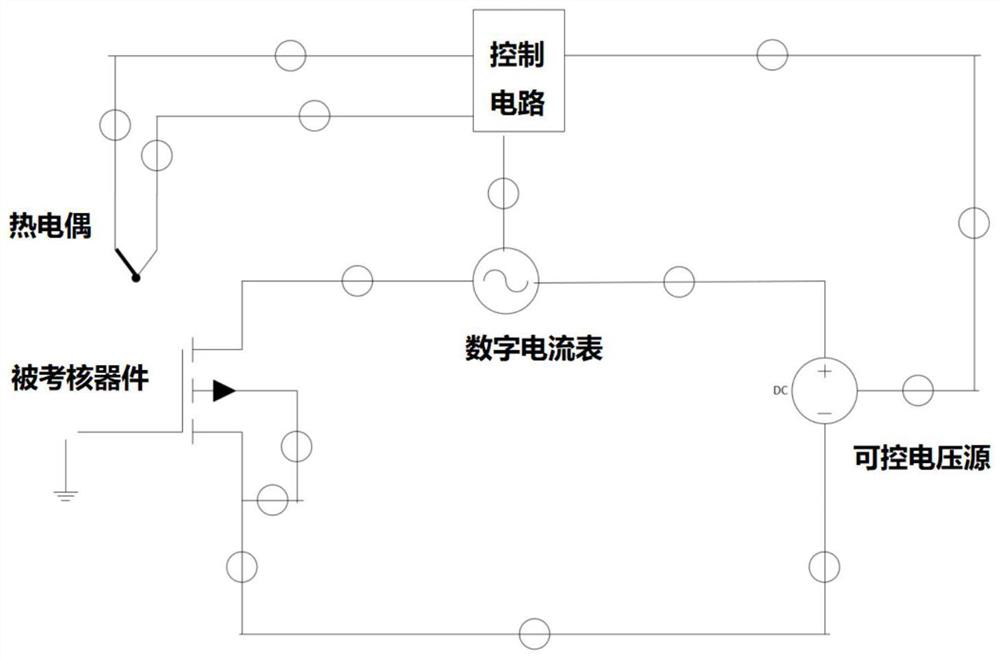
[0023] For ease of understanding, combine figure 2 As shown in the schematic diagram, the setting of the burn-in equipment and the VDMOS device to be aged in the burn-in equipment is firstly described.

[0024] Such as figure 2 As shown, the burn-in equipment includes: control circuit, thermocouple, digital ammeter and controllable voltage source.

[0025] The drain of the VDMOS device to be aged (the tested device shown in the figure) is connected to the positive pole of the controllable voltage source, the gate is connected to the negative pol...