Chip packaging module and electronic equipment
A chip packaging and module technology, applied in the direction of circuits, electrical components, electrical solid devices, etc., can solve the problem of easy delamination of conductive adhesive and carrier board, so as to alleviate the delamination phenomenon, stabilize the connection, and improve the structural stability Effect
- Summary
- Abstract
- Description
- Claims
- Application Information
AI Technical Summary
Problems solved by technology
Method used
Image

Examples
Embodiment Construction
[0021] In order to make the purpose, technical solution and advantages of the present application clearer, the technical solution of the present invention will be clearly and completely described below in conjunction with specific embodiments of the present invention and corresponding drawings. Apparently, the described embodiments are only some of the embodiments of the present invention, but not all of them. Based on the embodiments in this application, all other embodiments obtained by persons of ordinary skill in the art without making creative efforts belong to the scope of protection of this application.
[0022] The technical solutions disclosed in various embodiments of the present application will be described in detail below with reference to the accompanying drawings.
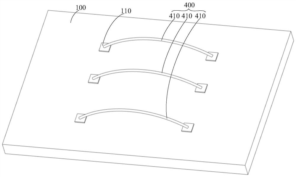
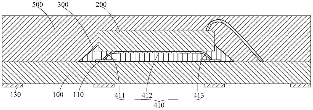
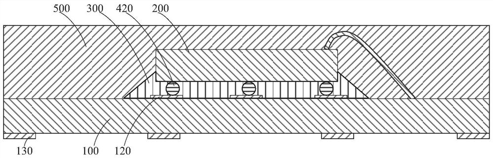
[0023] Please refer to Figure 1 to Figure 3 , the embodiment of the present application discloses a chip packaging module, which is applied to electronic equipment. The disclosed chip packaging mod...
PUM
 Abstract
Description
Claims
Application Information
 - R&D
- Intellectual Property
- Life Sciences
- Materials
- Tech Scout
- Unparalleled Data Quality
- Higher Quality Content
- 60% Fewer Hallucinations
Browse by: Latest US Patents, China's latest patents, Technical Efficacy Thesaurus, Application Domain, Technology Topic, Popular Technical Reports.
© 2025 PatSnap. All rights reserved.Legal|Privacy policy|Modern Slavery Act Transparency Statement|Sitemap|About US| Contact US: help@patsnap.com