
Broadband miniaturized antenna based on interactive embedded metasurface structure

A metasurface and embedded technology, applied in the direction of antenna, antenna grounding device, radiation element structure, etc., can solve the problems of metasurface antenna array design and integration difficulties, limited size reduction, large overall size, etc., to achieve cost and Effects of small weight, reduced size, and easy processing

Active Publication Date: 2020-12-04
SOUTH CHINA UNIV OF TECH
View PDF10 Cites 3 Cited by
  • Summary
  • Abstract
  • Description
  • Claims
  • Application Information

AI Technical Summary

Problems solved by technology

Compared with traditional microstrip patch antennas, metasurface antennas have obvious advantages in performance such as gain and bandwidth, but their overall size is usually larger (~1.1λ0), which leads to There are some difficulties in array design and integration of metasurface antennas
At present, the miniaturization methods of metasurface antennas generally include the following: adopt double-layer / multi-layer structure, reduce the gap between units, and use dielectric plates with high dielectric constant (W.E.I.Liu, Z.N.Chen, X. Qing, J.Shi and F.H.Lin, "Miniaturized wideband metasurface antennas," IEEE Transactions on Antennas and Propagation, vol.65, no.12, pp.7345-7349, Dec.2017.), loaded resonant structures (C. Zhao and C.Wang, "Characteristic mode design of wide band circularly polarized patch antenna consisting of H-shaped unit cells," IEEE Access, vol.6, pp.25292-25299, 2018.), increasing the current path (Y.Juan, W.Yang and W.Che, "Miniaturized low-profile circularly polarized metasurface antenna using capacitive loading," IEEE Transactions on Antennas and Propagation, vol.67, no.5, pp.3527-3532, May2019.), etc., but these The method usually has problems such as high profile, narrow bandwidth, and limited size reduction.

Method used


Image

  • Broadband miniaturized antenna based on interactive embedded metasurface structure
  • Broadband miniaturized antenna based on interactive embedded metasurface structure
  • Broadband miniaturized antenna based on interactive embedded metasurface structure

Examples


Embodiment

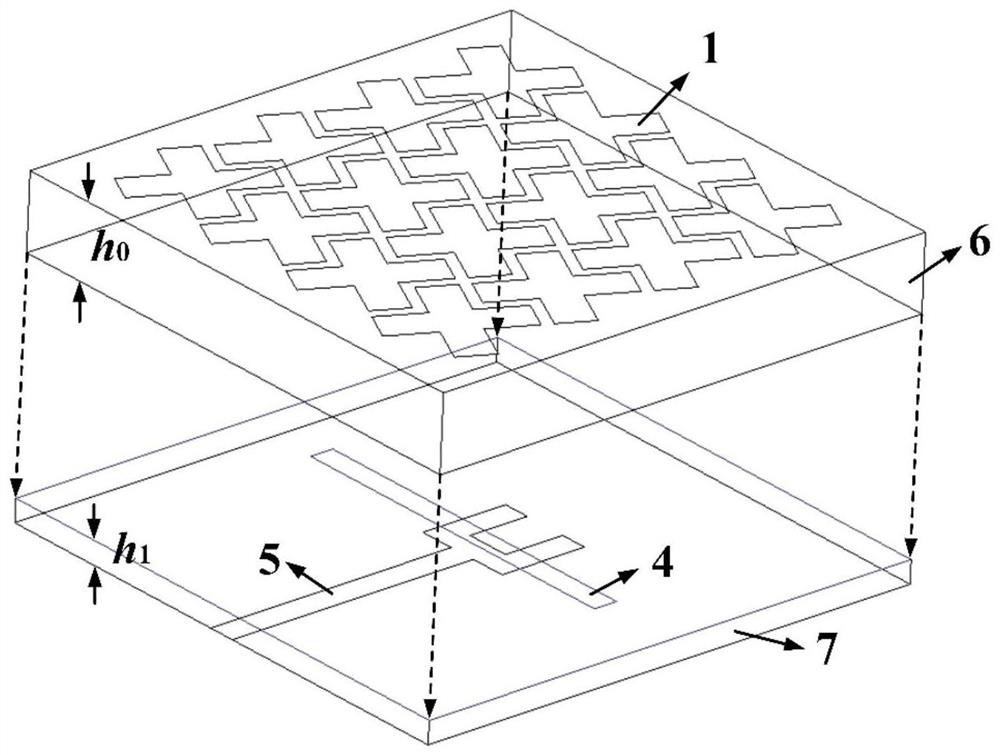
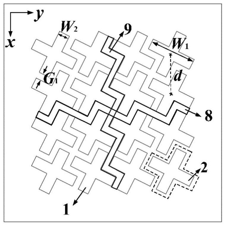
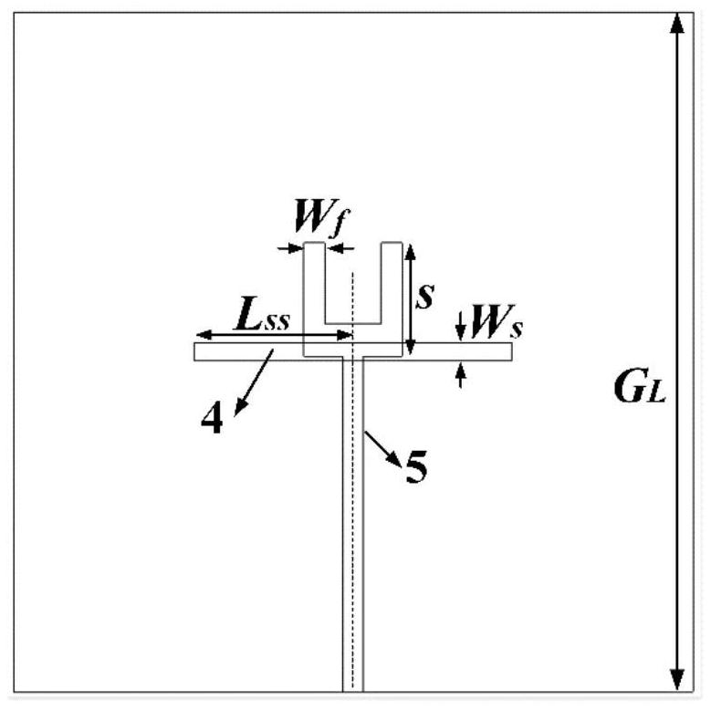
[0032] Such as Figure 1a , Figure 1b , Figure 1c , Figure 1d As shown, a broadband miniaturized antenna based on an interactive embedded metasurface structure includes an upper dielectric substrate 6 and a lower dielectric substrate 7, wherein the upper dielectric substrate 6 and the lower dielectric substrate 7 are placed in a double-layer stacked manner;

[0033] The dielectric constant of the upper dielectric substrate 6 is [2.2, 10.2], and the thickness h 0 is [0.001λ 0 ,0.1λ 0 ], the dielectric constant of the lower dielectric substrate 7 is [2.2,10.2], and the thickness h 1 Both are [0.001λ 0 ,0.1λ 0 ];

[0034] The upper surface of the upper dielectric substrate 6 is printed with an interactive embedded metasurface radiation structure 1, and the lower surface is printed with a metal floor 3 with a coupling gap 4; the upper surface of the lower dielectric substrate 7 is bonded to the metal floor 3, and the lower surface is printed There is a feeding network 5...


PUM


Abstract

The invention discloses a broadband miniaturized antenna based on an interactive embedded metasurface structure. The antenna comprises an upper-layer dielectric substrate and a lower-layer dielectricsubstrate which are placed in a double-layer stacking mode, wherein an interactive embedded metasurface radiation structure is printed on the upper surface of the upper dielectric substrate, a metal floor with a coupling gap is printed on the lower surface of the upper dielectric substrate, the upper surface of the lower dielectric substrate is attached to the metal floor, and the lower surface isprinted with a feed network. According to the invention, energy is input from a feed network and is coupled to an interactive embedded metasurface radiation structure through a coupling gap on a metal floor to directionally radiate the energy upwards, so that the miniaturized metasurface antenna with the characteristics of broadband, stability, high gain and low profile is realized; miniaturization is realized while the bandwidth is broadened; due to the diversity selection of the gap, the design freedom degree is improved while certain periodicity is guaranteed; and the antenna is simple instructure, easy to process, relatively low in cost and weight and capable of being produced on a large scale.

Description

technical field [0001] The invention relates to the field of metasurface antennas, in particular to a broadband miniaturized antenna based on an interactive embedded metasurface structure. Background technique [0002] With the development of modern wireless communication systems, the demand for wideband antennas is increasing. Microstrip patch antennas have attracted much attention due to their low profile, light weight, low cost, and easy compatibility with printed circuits. However, the traditional microstrip patch antenna has narrow impedance bandwidth and low gain. Although there are many technologies to overcome this shortcoming, such as using capacitive probe feeding, L probe feeding, aperture coupling, U / E open Groove patch and stack patch, etc., but usually require a thick dielectric substrate with a low dielectric constant, it is difficult to achieve a low profile (D.Chen, W.Yang, W.Che and Q.Xue, "Broadband stable-gain multiresonance antenna using nonperiodic sq...

Claims


Application Information

Patent Timeline
IPC IPC(8): H01Q1/38H01Q1/48H01Q1/50H01Q15/00
CPCH01Q1/38H01Q1/48H01Q1/50H01Q15/0086
Inventor 车文荃陈东旭杨琬琛薛泉
Owner SOUTH CHINA UNIV OF TECH
Learn More