
GOA circuit and display panel

A circuit and capacitor technology, applied in the field of GOA circuits and display panels, can solve the problems of low mobility, insufficient scanning signal potential, long charging time, etc., and achieve the effects of improving stability, maintaining stability, and reducing stress

Active Publication Date: 2020-12-08
WUHAN CHINA STAR OPTOELECTRONICS TECH CO LTD
View PDF7 Cites 5 Cited by
  • Summary
  • Abstract
  • Description
  • Claims
  • Application Information

AI Technical Summary

Problems solved by technology

[0002] When the display panel is displayed at a high frequency, due to the short charging time of the display area, the thin film transistor in the remote pixel has the problem of insufficient scanning signal potential due to the resistance and capacitance delay effect of the scanning line, especially for InGaZnO (IGZO) thin-film transistors, because the mobility of IGZO thin-film transistors is lower than that of low-temperature polysilicon (LTPS) thin-film transistors, and the charging time is longer, so compared with LTPS thin-film transistors, IGZO thin-film transistors need to improve their scanning. signal potential

Method used


Image

  • GOA circuit and display panel
  • GOA circuit and display panel
  • GOA circuit and display panel

Examples


Embodiment Construction

[0035] The technical solutions in the present application embodiment will be described in conjunction with the drawings in the present application embodiment. Obviously, the described embodiments are merely the embodiments of the present invention, not all of the embodiments. Based on the embodiments in the present application, those skilled in the art will belong to the scope of this application without all other embodiments obtained without creative labor.

[0036] The present application is distinguished all embodiments other than the thin film transistor gate poles, in which a source electrode is called, the other is called a drain electrode. Since the source and drain of the thin film transistor is symmetrical, so the source and drain are interchangeable. According to the shape of the figures of a predetermined intermediate gate terminal of the thin film transistor, a source signal input terminal, a signal output terminal is the drain. Furthermore, the present application all...


PUM


Abstract

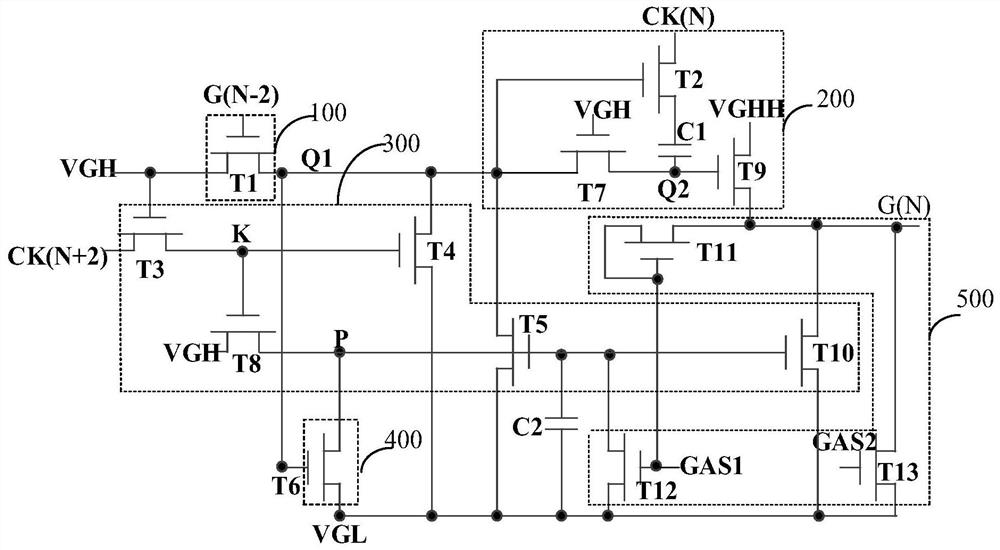
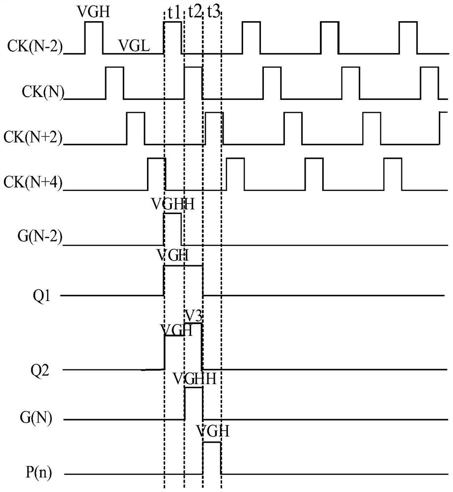
The invention provides a GOA circuit and a display panel. C1 and T2 are additionally arranged in a pull-up module of the GOA circuit, the potential of a Q2 point is increased through the coupling effect of C1, so that T9 is turned on more thoroughly, and then a second constant-voltage high potential higher than a first constant-voltage high potential is input from T9 and output as a scanning signal. Therefore, the potential of a scanning signal can be increased from the first constant-voltage high potential in the prior art to a second constant-voltage high potential, so that the potential ofthe scanning signal is increased, the requirement for increasing the potential of the scanning signal of an IGZO thin film transistor during high-frequency display in the LTPO technology can be met, and the synchronous requirement of the dynamic frame frequency technology for product vision and stability is met. The P point potential is still kept at the first constant-voltage high potential, so that the stability of the GOA circuit is kept, or when scanning signals with the same potential are output, the P point potential is lower, the stress borne by T5 and T10 is relieved, and the stabilityof the GOA circuit is improved.

Description

Technical field [0001] TECHNICAL FIELD The present application relates in particular to a circuit and a display panel GOA. Background technique [0002] At high frequencies the display panel, the display area due to the charging time is shorter, often delayed due to the capacitive effect of the resistance of the scanning line caused by the presence of the scanning signal potential problem of insufficient pixels in the distal end of the thin film transistor, especially for indium gallium zinc oxide (IGZO) thin film transistor, because the mobility of the thin film transistor of IGZO than the low-temperature polysilicon (LTPS) thin film transistor has low mobility, a long charging time, so compared to the LTPS TFT IGZO TFT, the need to improve its scan potential signal. [0003] For example, increasing the current low-temperature polycrystalline oxide hot (LTPO) display technology due to a combination of low temperature polysilicon (LTPS) thin film transistor and oxide (IGZO) thin ...

Claims


Application Information

Patent Timeline
Patent Type & Authority Applications(China)
IPC IPC(8): G09G3/20
CPCG09G3/20
Inventor 曹海明田超
Owner WUHAN CHINA STAR OPTOELECTRONICS TECH CO LTD
Learn More