Stable-clamping clamping mechanism for monocrystalline silicon wafer processing

A single crystal silicon wafer and clamping mechanism technology, which is applied in the directions of single crystal growth, single crystal growth, crystal growth, etc., can solve problems such as inconvenient placement, angle and direction adjustment of single crystal silicon rods, and inability to ensure clamping stability. Achieve the effect of avoiding slipping and adjusting the angle

Inactive Publication Date: 2020-12-18
江苏晶品新能源科技有限公司
View PDF8 Cites 2 Cited by
  • Summary
  • Abstract
  • Description
  • Claims
  • Application Information

AI Technical Summary

Problems solved by technology

[0005] Aiming at the deficiencies of the prior art, the present invention provides a clamping mechanism for single crystal silicon wafer processing with stable clamping, which has the advantages of stable clamping and angle adjustment, and solves the problem that single crystal silicon wafers are processed by single crystal silicon rods. It is cut by a series of proces

Method used


Image

  • Stable-clamping clamping mechanism for monocrystalline silicon wafer processing
  • Stable-clamping clamping mechanism for monocrystalline silicon wafer processing
  • Stable-clamping clamping mechanism for monocrystalline silicon wafer processing

Examples


Embodiment Construction

[0024] The following will clearly and completely describe the technical solutions in the embodiments of the present invention with reference to the accompanying drawings in the embodiments of the present invention. Obviously, the described embodiments are only some, not all, embodiments of the present invention. Based on the embodiments of the present invention, all other embodiments obtained by persons of ordinary skill in the art without making creative efforts belong to the protection scope of the present invention.

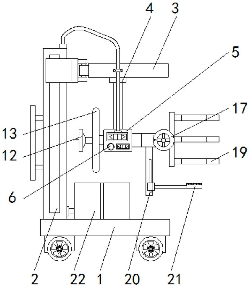
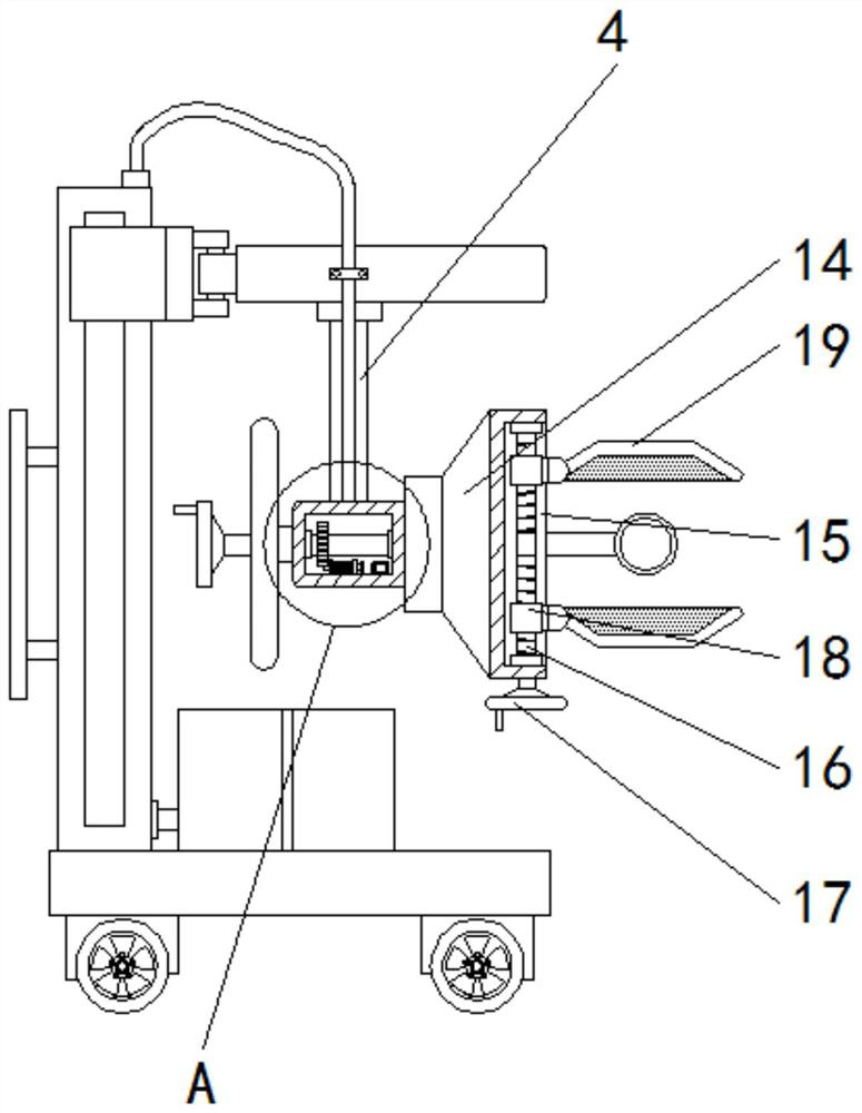
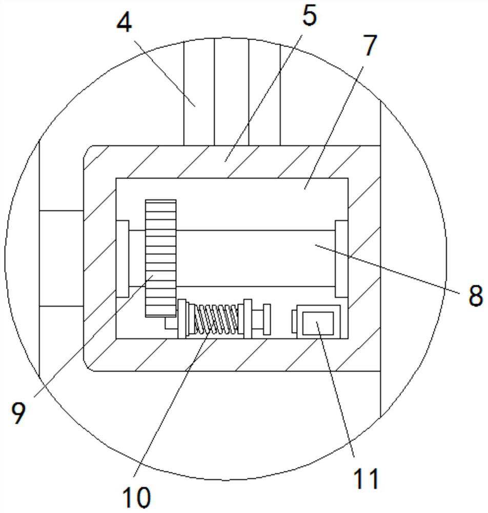
[0025] see Figure 1-3, a clamping mechanism for processing monocrystalline silicon wafers with stable clamping, including a mobile base 1, two brake-type mobile wheels are fixedly installed on the front and rear sides of the bottom of the mobile base 1, and the left side of the top of the mobile base 1 The first electric sliding table 2 is fixedly installed, and the left side of the first electric sliding table 2 is fixedly connected with a push rod, and the ...


PUM


Abstract

The invention relates to the technical field of monocrystalline silicon wafer processing, and discloses a stable-clamping clamping mechanism for monocrystalline silicon wafer processing. The stable-clamping clamping mechanism comprises a moving base, a first electric sliding table is fixedly installed on the left side of the top of the moving base, and a sliding block of the first electric slidingtable is rotatably connected with a rotating plate located on the right side of the first electric sliding table; and a connecting rod is slidably connected to the bottom of the rotating plate, a connector is fixedly connected to the bottom of the connecting rod, and a control device is fixedly installed on the front side of the connector. The stable-clamping clamping mechanism for monocrystalline silicon wafer processing solves the problems that a monocrystalline silicon wafer is formed by cutting a monocrystalline silicon rod through a series of processes, the monocrystalline silicon rod needs to be clamped when being taken out of a single crystal furnace, but an existing clamping mechanism only clamps the monocrystalline silicon rod through friction force in the clamping process, clamping stability cannot be guaranteed, the angle direction of the monocrystalline silicon rod cannot be adjusted after the monocrystalline silicon rod is clamped and taken out, so that the monocrystalline silicon rod is inconvenient to place.

Description

technical field [0001] The invention relates to the technical field of monocrystalline silicon wafer processing, in particular to a clamping mechanism for monocrystalline silicon wafer processing with stable clamping. Background technique [0002] Monocrystalline silicon wafer is a single crystal of silicon, which is a crystal with a basically complete lattice structure. Different directions have different properties. It is a good semiconducting material, used in the manufacture of semiconductor devices, solar cells, etc. High-purity polycrystalline silicon is drawn in a single crystal furnace. Monocrystalline silicon is a relatively active non-metallic element and an important part of crystal materials. It is at the forefront of new material development. Its main purpose is to be used as a semiconductor material And the use of solar photovoltaic power generation, heating and so on. [0003] Single crystal silicon wafers are cut from single crystal silicon rods through a se...

Claims


Application Information

Patent Timeline
IPC IPC(8): C30B35/00C30B29/06
CPCC30B29/06C30B35/00
Inventor 陈春成戚建静
Owner 江苏晶品新能源科技有限公司
Why Eureka
Try Eureka