Display panel, manufacturing method thereof and display device

A display panel and manufacturing method technology, applied in semiconductor/solid-state device manufacturing, organic semiconductor devices, electrical components, etc., capable of solving problems such as poor display effect

Pending Publication Date: 2020-12-18
HEFEI XINSHENG OPTOELECTRONICS TECH CO LTD +1
View PDF7 Cites 6 Cited by
  • Summary
  • Abstract
  • Description
  • Claims
  • Application Information

AI Technical Summary

Problems solved by technology

The problem of poor display effect of OLED display panels in the prior art can be solved, and the technical solution is as follows:

Method used


Image

  • Display panel, manufacturing method thereof and display device
  • Display panel, manufacturing method thereof and display device
  • Display panel, manufacturing method thereof and display device

Examples


Embodiment Construction

[0070] In order to make the purpose, technical solution and advantages of the present application clearer, the implementation manners of the present application will be further described in detail below in conjunction with the accompanying drawings.

[0071] In the related art, in order to avoid the problem that the organic light-emitting material is easily attached to the auxiliary electrode when the organic light-emitting material is evaporated, which will affect the electrical connection between the auxiliary electrode and the subsequently formed cathode layer.

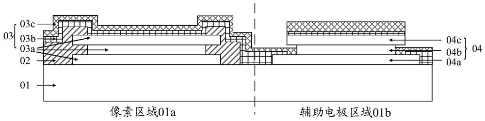
[0072] For this, please refer to figure 1 , figure 1 It is a schematic diagram of the film layer structure of an OLED display panel provided by the related art. The OLED display panel may include: a substrate 01 , and a pixel defining layer 02 , an OLED light emitting device 03 and an auxiliary electrode layer 04 located on the substrate 01 . Wherein, the pixel defining layer 02 is used to define a pixel area 01 ...


PUM

PropertyMeasurementUnit
thicknessaaaaaaaaaa

Abstract

The invention discloses a display panel, a manufacturing method thereof and a display device, and belongs to the technical field of display. The method comprises the following steps: sequentially forming a conductive pattern, a light-emitting layer and a cathode layer on a substrate, wherein the conductive pattern can comprise an anode layer and an auxiliary electrode layer, and the auxiliary electrode layer comprises a first protection electrode, a metal electrode and a second protection electrode which are stacked in the direction perpendicular to and away from the substrate. The second protection electrode and the first protection electrode protrude out of the metal electrode in the direction parallel to the substrate, so that when the light-emitting layer is formed on the second protection electrode, the light-emitting layer is only attached to the second protection electrode and the edge area of the first protection electrode; therefore, the subsequently formed cathode layer can be in contact with the side wall of the metal electrode and the first protection electrode, and the display effect of the display panel is good.

Description

technical field [0001] The present application relates to the field of display technology, in particular to a display panel, a manufacturing method thereof, and a display device. Background technique [0002] The current organic electroluminescent (English: Organic Light-Emitting Diode abbreviation: OLED) display panel usually includes an anode layer, an organic light-emitting layer and a cathode layer, which can be divided into bottom-emitting OLED display panels and top-emitting OLEDs according to different light-emitting surfaces. There are two types of display panels. Since the top emission OLED display panel can obtain a larger aperture ratio, it has become a research hotspot in recent years. [0003] Top-emission OLED display panels require a thin and transparent cathode layer and an anode layer capable of light reflection to increase light transmittance, and a thin and transparent cathode layer generally has a high resistance value and a voltage drop (IR drop) seriou...

Claims


Application Information

Patent Timeline
Patent Type & Authority Applications(China)
IPC IPC(8): H01L51/52H01L51/56H01L27/32
CPCH10K59/12H10K50/824H10K71/00H10K59/122H10K71/621H10K50/813H10K50/818H10K2102/3026H10K50/84H10K50/814
Inventor 张扬刘宁周斌程磊磊闫梁臣刘军王庆贺孙涛罗志文
Owner HEFEI XINSHENG OPTOELECTRONICS TECH CO LTD
Why Eureka
Try Eureka