A kind of igbt device and its manufacturing process

A manufacturing process and device technology, applied in the field of power semiconductors, can solve the problems of increased saturation voltage drop, decreased current density, loss of chip area, etc., to achieve the effect of balanced saturation voltage drop, balanced current density, and enhanced short-circuit capability

Active Publication Date: 2022-06-28
JIANGSU HAIDONG SEMICON TECH CO LTD
View PDF8 Cites 0 Cited by
  • Summary
  • Abstract
  • Description
  • Claims
  • Application Information

AI Technical Summary

Problems solved by technology

[0004] In order to achieve the same current specification, the cell pitch with the dummy structure usually increases proportionally. Under the same current specification, the chip area of ​​the dummy structure IGBT is usually twice that of the non-dummy structure; the chip area is lost under the same short-circuit capability, resulting in an increase in cost. High; the same chip area causes a decrease in current density and an increase in saturation voltage drop

Method used


Image

  • A kind of igbt device and its manufacturing process
  • A kind of igbt device and its manufacturing process
  • A kind of igbt device and its manufacturing process

Examples


Embodiment Construction

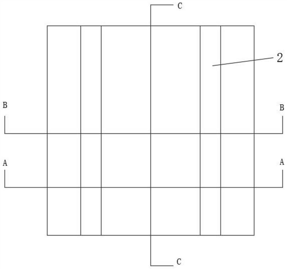
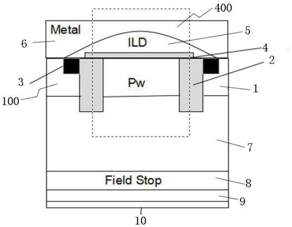
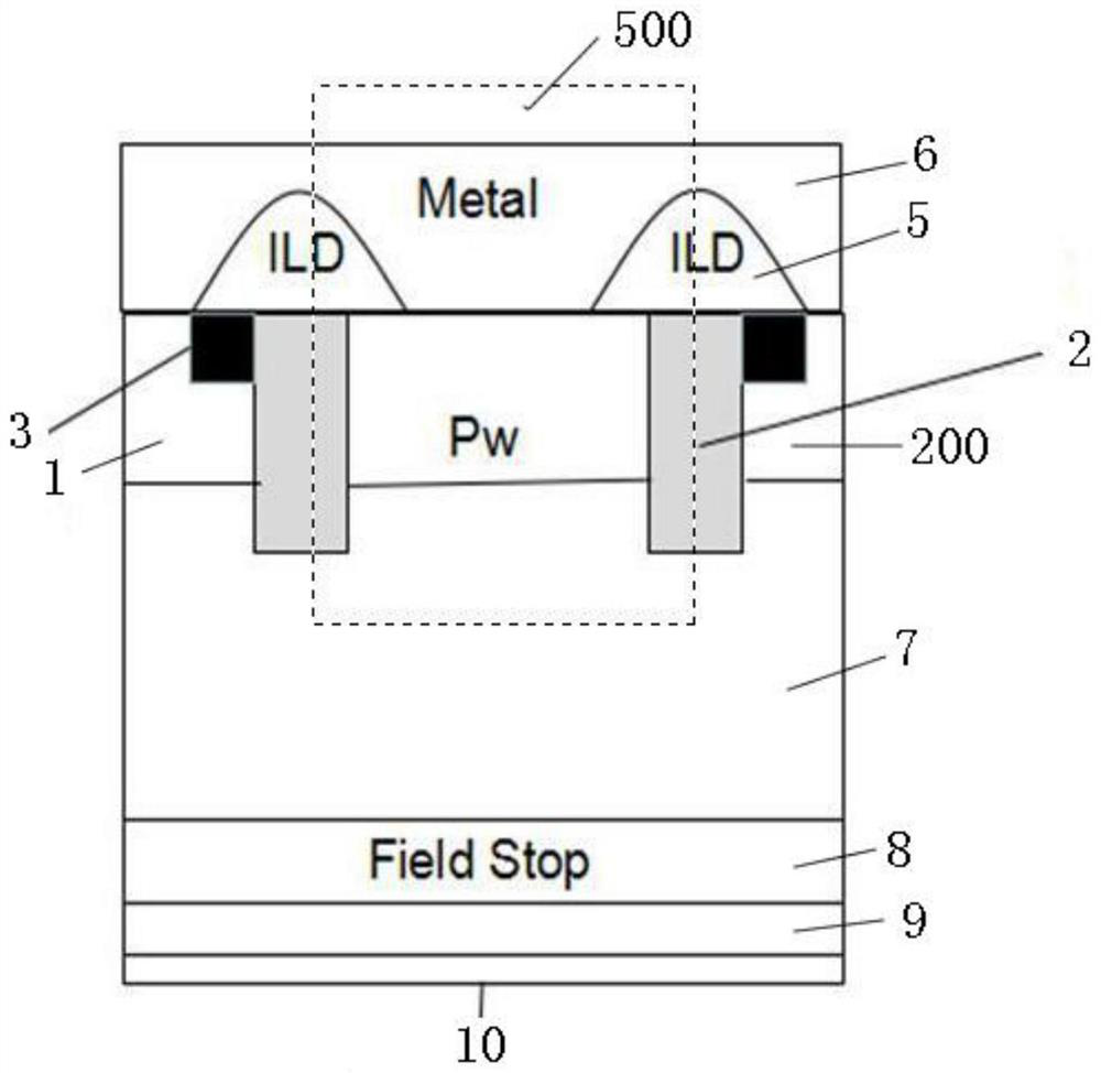
[0045]The following detailed description is made with reference to the accompanying drawings, which form a part hereof, and in which the accompanying drawings are shown by way of explanation of specific embodiments for implementing the invention. It is to be understood that other embodiments may be utilized and structural or logical changes may be made without departing from the scope of the present invention. For example, features explained or described for one embodiment can be used or combined with other embodiments to yield yet another embodiment. It is intended that the present invention includes such modifications and variations. These examples are described with specific language, but they should not be construed as limiting the scope of the appended claims. The drawings are for explanatory purposes only and are not drawn to scale. For the sake of clarity, corresponding elements have been designated by the same reference numerals in the different figures unless otherw...


PUM

PropertyMeasurementUnit
electrical resistivityaaaaaaaaaa

Abstract

The present invention provides an IGBT device, which has good short-circuit capability and can reduce the saturation voltage drop of the IGBT device and increase the current density, comprising a semiconductor substrate and cells arranged on the semiconductor substrate, and the cells include The effective cell and the virtual cell are characterized in that: on the cross section of the IGBT device, the effective cell includes: a first effective cell, a second effective cell, and a third effective cell, and the virtual cell includes : a first virtual cell, a second virtual cell, the first virtual cell is separated from the first effective cell by a trench gate, the second virtual cell is separated from the second effective cell Cells are separated by trench gates.

Description

technical field [0001] The invention belongs to the technical field of power semiconductors, and in particular relates to an IGBT device, and the invention also relates to a manufacturing process of the IGBT device. Background technique [0002] IGBT (INsulated Gate BiPolar TraNsistor), insulated gate bipolar transistor, is a composite fully controlled voltage-driven power semiconductor device composed of BJT (bipolar transistor) and MOS (insulated gate field effect transistor), and also has MOSFET advantages of high input impedance and low on-voltage drop of GTR. The GTR saturation voltage is reduced, the current carrying density is large, but the driving current is large; the MOSFET driving power is small, the switching speed is fast, but the on-state voltage drop is large, and the current carrying density is small. The IGBT combines the advantages of the above two devices, and the driving power is small and the saturation voltage is reduced. It is very suitable for conv...

Claims


Application Information

Patent Timeline
Patent Type & Authority Patents(China)
IPC IPC(8): H01L29/739H01L29/423H01L21/331
CPCH01L29/66348H01L29/7397H01L29/4236
Inventor 赵家宽夏华秋夏华忠谈益民吕文生黄传伟
Owner JIANGSU HAIDONG SEMICON TECH CO LTD
Why Eureka
Try Eureka