Silicon wafer adsorption unit and silicon wafer transmission device

A technology of adsorption unit and silicon wafer, which is applied in the direction of transportation and packaging, electrical components, conveyor objects, etc., can solve the problem of large space occupation, achieve the effect of simplifying the delivery path, ensuring timeliness and reliability

Pending Publication Date: 2020-12-29
BEIJING U PRECISION TECH
View PDF0 Cites 2 Cited by
  • Summary
  • Abstract
  • Description
  • Claims
  • Application Information

AI Technical Summary

Problems solved by technology

[0004] The first object of the present invention is to provide a silicon wafer adsorption unit to solve the technical problem that the existing silicon wafer transport device occupies a large space

Method used


Image

  • Silicon wafer adsorption unit and silicon wafer transmission device
  • Silicon wafer adsorption unit and silicon wafer transmission device
  • Silicon wafer adsorption unit and silicon wafer transmission device

Examples


Embodiment Construction

[0039] In order to make the above objects, features and advantages of the present invention more comprehensible, specific embodiments of the present invention will be described in detail below in conjunction with the accompanying drawings. It should be understood that the specific embodiments described here are only used to explain the present invention, not to limit the present invention.

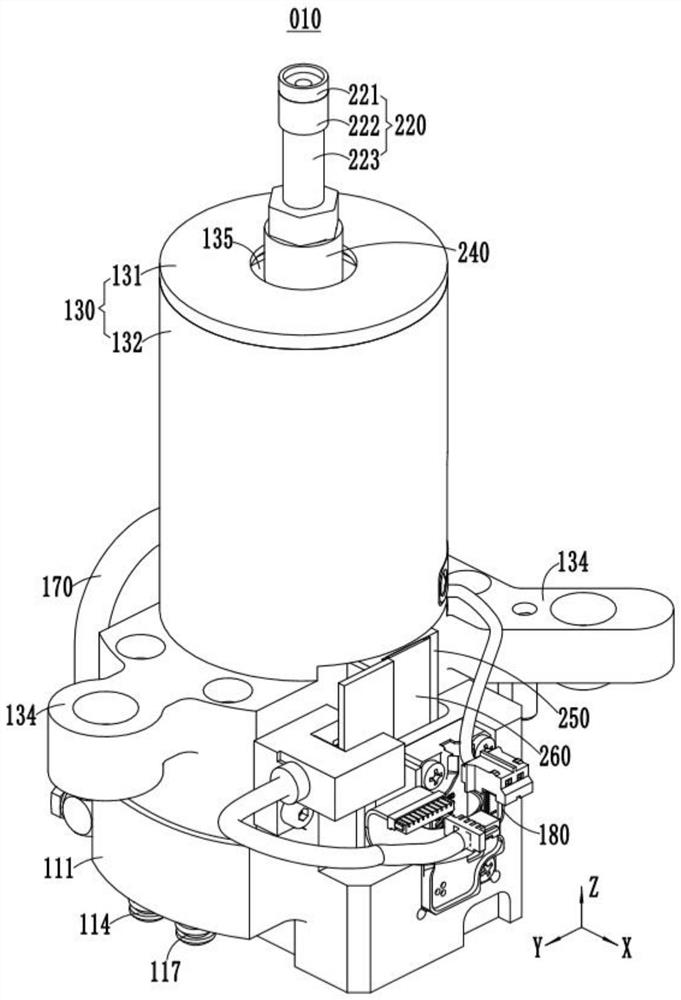
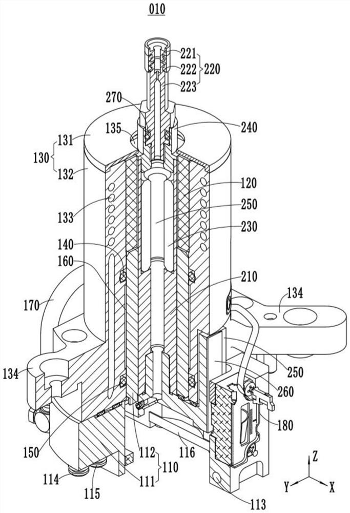
[0040] figure 2 A schematic structural diagram of the silicon wafer adsorption unit 010 provided in this embodiment, image 3 A cross-sectional view of a partial structure of the silicon wafer adsorption unit 010 provided in this embodiment. Such as figure 2 with image 3 As shown, this embodiment provides a silicon wafer adsorption unit 010, including a stator assembly and a mover assembly, specifically, the stator assembly includes a base 110, and the base 110 is provided with a guide part; the mover assembly includes a moving part and an adsorption The head 220, wherein the moving...


PUM


Abstract

The invention provides a silicon wafer adsorption unit and a silicon wafer transmission device and relates to the technical field of semiconductor manufacturing equipment, and the device is designed for solving the problem that an existing silicon wafer transmission device is large in occupied space. The silicon wafer adsorption unit comprises a stator assembly and a rotor assembly, the stator assembly comprises a base, and the base is provided with a guide part; the rotor assembly comprises a moving part and an adsorption head, the moving part and the guide part are matched in an inserted mode, and a circumferential limiting structure for limiting relative rotation of the moving part and the guide part is arranged between the moving part and the guide part; the adsorption head is fixed arranged on the moving part, the adsorption head and the moving part are arranged in the insertion direction of the moving part and the guide part. The silicon wafer transmission device comprises the silicon wafer adsorption unit. According to the silicon wafer adsorption unit and the silicon wafer transmission device provided by the invention, a rotation limiting structure arranged in the lateral direction of suction cups in a multi-suction-cup integrated structure in the prior art is omitted, so that the overall structure of the silicon wafer adsorption unit is compact.

Description

technical field [0001] The invention relates to the technical field of semiconductor manufacturing equipment, in particular to a silicon wafer adsorption unit and a silicon wafer transport device. Background technique [0002] With the development of the semiconductor industry, the overall structure of the lithography machine workpiece table is becoming more and more complex. Under the limitation of the overall size, higher requirements are placed on the compactness of each component. Usually, the transfer and transportation of the silicon wafer 70 is realized by a silicon wafer transport device. Specifically, such as figure 1 As shown, the silicon wafer transfer device includes a base 10, a driving mechanism 20, a guide mechanism 30, a connecting plate 40 and a plurality of suction cups 50, wherein the driving mechanism 20 is provided in multiple groups, and each group of driving mechanisms 20 includes a The stator 22 of 10 and the mover 21 that can move up and down relat...

Claims


Application Information

Patent Timeline
Patent Type & Authority Applications(China)
IPC IPC(8): H01L21/683H01L21/677
CPCH01L21/67709H01L21/6838
Inventor 杜欣宇金实张利
Owner BEIJING U PRECISION TECH
Why Eureka
Try Eureka