A clamping and processing device for pcb board processing in the production process of electronic parts

A production process and PCB board technology, which is applied in the direction of assembling printed circuits, electrical components, electrical components, etc., can solve problems such as difficult to take out, difficult to adapt to different specifications of boards, and easy to be absorbed by workers, reaching the scope of applicability wide, protect the health, reduce the effect of dust residue

Active Publication Date: 2021-06-22
SUZHOU ODIHUA ELECTRONIC CO LTD
View PDF0 Cites 0 Cited by
  • Summary
  • Abstract
  • Description
  • Claims
  • Application Information

AI Technical Summary

Problems solved by technology

[0004] The purpose of the embodiments of the present invention is to provide a PCB board processing and clamping device in the production process of electronic parts that has wide applicability, is easy to remove the board, and can purge the dust. It is fixed, but the existing device is difficult to adapt to different specifications of boards in terms of fixing. Facing boards of different sizes, only the fixture can be replaced, which is very inconvenient, and because the thickness of the PCB board is very small, it is not easy to fix it after processing. It is taken out, and a large amount of dust will be generated during the processing, which is easily absorbed by workers and affects the health of workers

Method used


Image

  • A clamping and processing device for pcb board processing in the production process of electronic parts
  • A clamping and processing device for pcb board processing in the production process of electronic parts
  • A clamping and processing device for pcb board processing in the production process of electronic parts

Examples


Embodiment 1

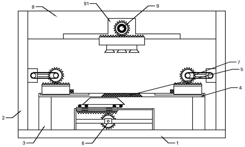
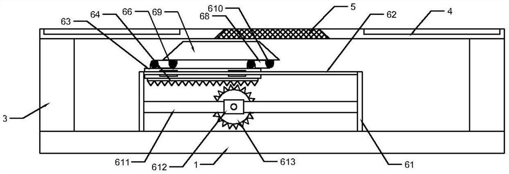
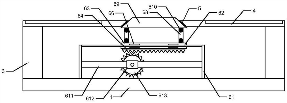
[0028] Such as Figure 2 to Figure 5 As shown, in the embodiment of the present invention, the jacking device 6 includes a support frame 61, the support frame 61 is fixedly installed on the bottom plate 1 between the support columns 3, and the top of the support frame 61 is installed with a square frame 62, the inside of the square frame 62 is provided with a first slide plate 63, the bottom of the first slide plate 63 is equipped with a first rack 64, the side of the first slide plate 63 has a control groove 65, and the control groove 65 The inner bearing is connected with a roller 66, the side of the roller 66 is provided with an engaging groove 67, the engaging groove 67 is matched with the side bar of the square frame 62, and a first connecting rod 68 is hinged above the first slide plate 63, The other end of the first connecting rod 68 is hinged with a push plate 69, and the first slide plate 63 and the first connecting rod 68 are hinged and the first connecting rod 68 an...

Embodiment 2

[0034] Such as Figure 8 As shown, in the embodiment of the present invention, the fixing device 7 includes a mounting block 71, the mounting block 71 is fixedly installed on both sides inside the frame 2, and a fixing rod 72 is installed on the side of the mounting block 71, the The other end of the fixed rod 72 is hinged with a second gear 73, the middle part of the second gear 73 is fixed with a first turntable 74, the mounting block 71 is equipped with a second motor 75, and the second motor 75 is equipped with a first Two turntables 76, an interlocking belt 77 is arranged between the first turntable 74 and the second turntable 76; a first chute 78 is provided on both sides of the placement plate 4, and a first chute 78 is provided inside the first chute 78. A slider 79 , a second rack 710 is mounted on the top of the first slider 79 , and the second rack 710 meshes with the second gear 73 .

[0035] During use, the plate is placed on the placement plate 4, and then the s...

Embodiment 3

[0038] Such as Figure 6 and Figure 7 As shown, in the embodiment of the present invention, the purging device 9 includes a control groove 91, the control groove 91 is opened inside the top plate 8, and a third motor 92 is fixedly installed on the inner wall of the control groove 91, and the third motor 92 A second connecting rod 93 is fixedly installed on the motor 92, and a third connecting rod 94 is hinged at the other end of the second connecting rod 93; a communication groove 95 is opened in the wall of the control groove 91, and the other side of the communication groove 95 The bearing is connected with an inner screw nut 96, and an outer screw rod 97 is arranged inside the inner screw nut 96. One end of the outer screw rod 97 close to the inside of the control groove 91 is hinged with the third connecting rod 94. The inner screw nut 96 A gear ring 98 is installed on the outer side; a second chute 99 is opened at the bottom of the communication groove 95, and a second ...


PUM


Abstract

The present invention is applicable to the field of electronic parts production, and provides a PCB board processing and clamping device in the production process of electronic parts, including: a bottom plate, a frame is installed above the bottom plate, and a support is installed inside the frame above the bottom plate column, a placement plate is installed above the support column, and a push groove is opened on the placement plate, a jacking device is installed between the support columns below the placement plate, and a fixing device is installed between the placement plate and the frame device, a top plate is installed on the top of the frame, and a purging device is installed inside the top plate. By modifying the fixing device, the fixing device can be automatically adapted according to the different sheet specifications, so that the applicability range of the device Widen, and at the same time add a jacking device, so that the processed plate can be automatically lifted up to facilitate the removal of the plate, and a blowing device is installed to blow the plate to the greatest extent through left and right reciprocating movements, reducing air pollution. of dust residue.

Description

technical field [0001] The invention belongs to the field of electronic parts production, and in particular relates to a PCB board processing and clamping device in the production process of electronic parts. Background technique [0002] Printed circuit boards, also known as printed circuit boards, are providers of electrical connections for electronic components. Printed circuit boards are mostly represented by "PCB". Its development has a history of more than 100 years; its design is mainly layout design; the main advantage of using circuit boards is that it greatly reduces wiring and assembly errors, and improves automation and production labor rates. According to the number of layers of circuit boards, it can be divided into single-sided boards, double-sided boards, four-layer boards, six-layer boards and other multi-layer circuit boards. Since the printed circuit board is not a general terminal product, the definition of the name is slightly confusing. They are not ...

Claims


Application Information

Patent Timeline
Patent Type & Authority Patents(China)
IPC IPC(8): H05K3/00H05K3/32H05K13/00B08B5/02
CPCH05K3/00H05K3/32H05K13/0069B08B5/02
Inventor 费城
Owner SUZHOU ODIHUA ELECTRONIC CO LTD
Why Eureka
Try Eureka