Wafer centering mechanism, wafer transmission device and wafer thinning equipment

A centering mechanism and wafer technology, applied in transportation and packaging, grinding drive devices, metal processing equipment, etc., can solve problems such as failure of manipulators to pick and place wafers, insufficient vacuum pressure of suction cups, etc., to ensure concentricity and surface The effect of improving quality and reliability

Active Publication Date: 2021-01-08
HWATSING TECH
View PDF11 Cites 13 Cited by
  • Summary
  • Abstract
  • Description
  • Claims
  • Application Information

AI Technical Summary

Problems solved by technology

When the wafer position deviates from the preset position, failures such as failure of the manipulator to pick and place wafers will occur
[0004] During the wafer grinding process, the wafer needs to be transferred from the transfer device to the grinding table. When there is a deviation between the center of the wafer and the center of the transfer device, the wafer transfer robot will also bring the deviation to the grinding table Above; Generally, the grinding table is a ceramic suction cup structure, and the suction area of ​​the suction cup is close to the diameter of the wafer. Once there is a deviation between the center of the wafer and the center of the grinding table, the vacuum pressure of the suction cup will be insufficient. More serious accidents such as slides

Method used


Image

  • Wafer centering mechanism, wafer transmission device and wafer thinning equipment
  • Wafer centering mechanism, wafer transmission device and wafer thinning equipment
  • Wafer centering mechanism, wafer transmission device and wafer thinning equipment

Examples


Embodiment Construction

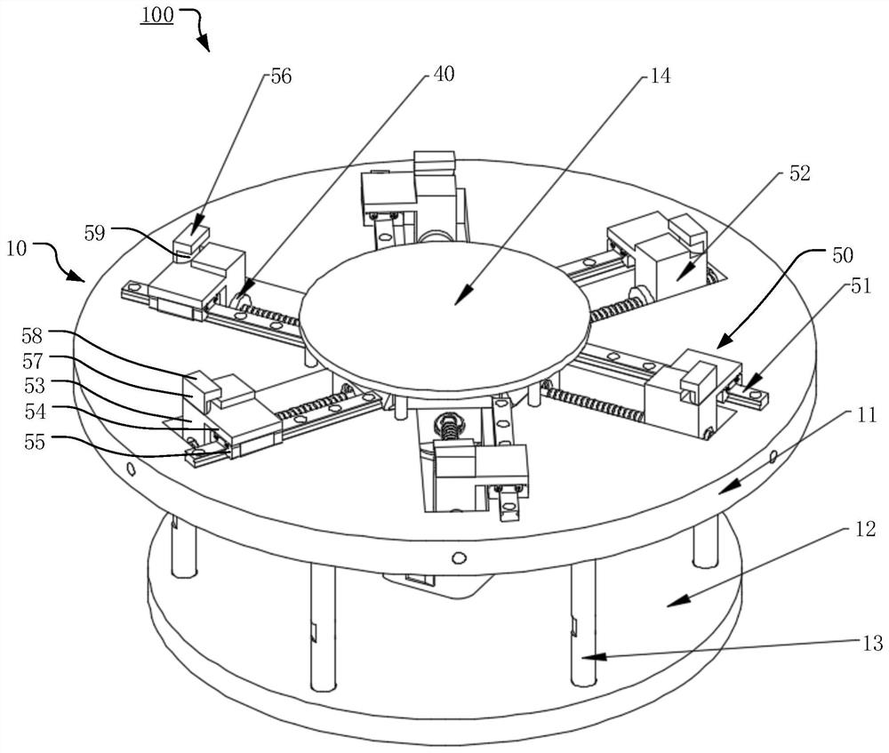
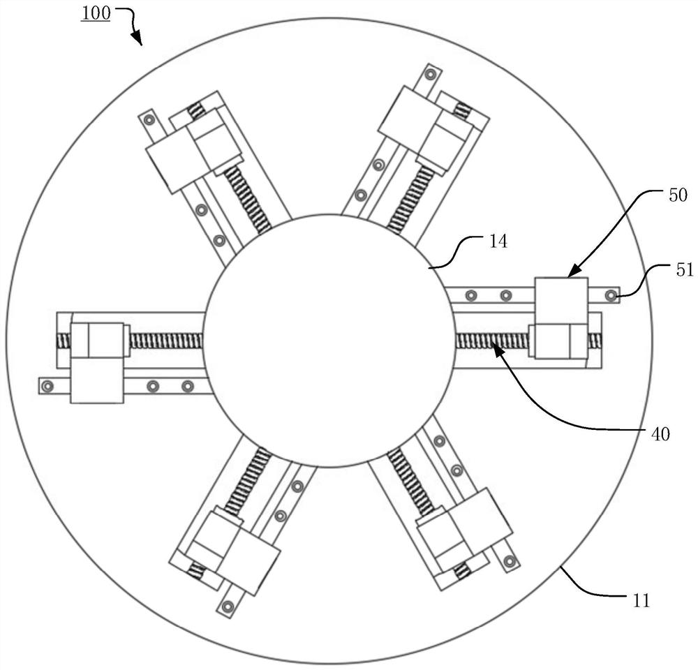
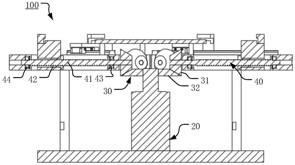
[0033] The technical solutions of the present invention will be described in detail below in conjunction with specific embodiments and accompanying drawings. The examples described here are specific implementations of the present invention and are used to illustrate the concept of the present invention; these descriptions are all explanatory and exemplary, and should not be construed as limiting the implementation of the present invention and the protection scope of the present invention . In addition to the embodiments described here, those skilled in the art can also adopt other obvious technical solutions based on the claims of the application and the contents disclosed in the specification, and these technical solutions include adopting any modifications made to the embodiments described here. Obvious alternatives and modified technical solutions. It should be understood that, unless otherwise specified, for ease of understanding, the following descriptions of the specifi...


PUM


Abstract

The invention discloses a wafer centering mechanism, a wafer conveying device and wafer thinning equipment. The wafer centering mechanism comprises a fixed table, a rotary driving mechanism, a bevel gear assembly, a preset number of ball screw assemblies and a preset number of movable clamping assemblies, wherein the preset number of ball screw assemblies are evenly installed on the fixed table inthe circumferential direction and arranged in the horizontal direction, the linear motion ends of the ball screw assemblies are connected with the mobile clamping assemblies, the ball screw assemblies are located on the periphery of the bevel gear assembly, the rotating ends of the ball screw assemblies are fixedly connected with the bevel gear assembly, and the bevel gear assembly is fixedly connected with the rotary driving mechanism located below the bevel gear assembly.

Description

technical field [0001] The invention relates to the technical field of wafer thinning, in particular to a wafer centering mechanism, a wafer transmission device and wafer thinning equipment. Background technique [0002] At present, the semiconductor industry uses electronic circuits such as IC (Integrated Circuit, integrated circuit) or LSI (Large Scale Integration, large scale integrated circuit) formed on the surface of the semiconductor wafer to manufacture semiconductor chips. Before the wafer is divided into semiconductor chips, the wafer is ground to a predetermined thickness by grinding the back surface of the wafer opposite to the device surface on which the electronic circuit is formed. [0003] Wafer alignment control is one of the important links in the integrated circuit manufacturing process. During the process of wafer transfer at each station, higher requirements are required for its position. When the wafer position deviates from the preset position, failu...

Claims


Application Information

Patent Timeline
Patent Type & Authority Applications(China)
IPC IPC(8): H01L21/68H01L21/677H01L21/67B24B19/22B24B29/02B24B27/00B24B41/00B24B47/22
CPCH01L21/68H01L21/67703H01L21/67092B24B19/22B24B29/02B24B27/0023B24B41/005B24B47/22
Inventor 刘远航马旭王江涛赵德文
Owner HWATSING TECH
Why Eureka
Try Eureka