

Brushless motor driving circuit and method
A brushless motor and drive circuit technology, applied in the direction of a single motor speed/torque control, starting device, etc., can solve problems such as affecting the normal operation of the equipment, large starting current, accelerated motor aging, etc., to avoid excessive bus voltage. , Improve the service life and reduce the effect of starting current
- Summary
- Abstract
- Description
- Claims
- Application Information
AI Technical Summary
Problems solved by technology
Method used
Image

Examples
Embodiment Construction
[0021] The present invention is described in further detail below in conjunction with accompanying drawing:
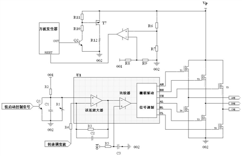
[0022] Such as figure 1 Shown is the brushless motor driving circuit of the present invention, including a soft-start delay speed regulation circuit, a bus voltage suppression circuit and a three-phase bridge inverter circuit.
[0023] 001 is the positive terminal of the voltage source power supply, and 002 is the negative terminal of the voltage source power supply.
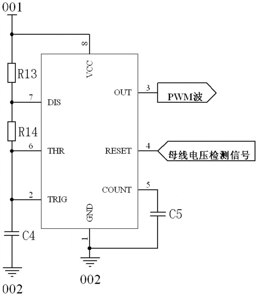
[0024] The soft start delay speed regulating circuit includes transistor Q1, capacitor C1, capacitor C2, capacitor C3, adjustable resistor R1, resistor R2, resistor R3, resistor R4, resistor R5, motor control chip U1 and motor adapter.
[0025] The soft start control signal is connected to the base of the transistor Q1, the emitter of the transistor Q1 is connected to the first terminal of the capacitor C1, the first terminal of the adjustable resistor R1 is connected to the negative terminal of the vol...
PUM
 Abstract
Description
Claims
Application Information