Pressure module and manufacturing method thereof

A technology of pressure module and manufacturing method, which is applied in the manufacture of microstructure devices, piezoelectric/electrostrictive/magnetostrictive devices, piezoelectric effect/electrostrictive or magnetostrictive motors, etc., can solve the problem of MEMS chip bonding problems such as disconnection, affecting system reliability, and high maintenance costs

Pending Publication Date: 2021-01-15
华景传感科技(无锡)有限公司
View PDF0 Cites 1 Cited by
  • Summary
  • Abstract
  • Description
  • Claims
  • Application Information

AI Technical Summary

Problems solved by technology

[0004] In the prior art, the packaging structure of the MEMS chip and the ASIC chip in the general sensor module is to directly attach and fix the two relative to each other through adhesive layer bonding or welding. In this way, during the use of the sensor module, there will be leakage of the chip seal. Especially in

Method used


Image

  • Pressure module and manufacturing method thereof
  • Pressure module and manufacturing method thereof
  • Pressure module and manufacturing method thereof

Examples


Embodiment Construction

[0040] In order to make the object, technical solution and advantages of the present invention clearer, specific embodiments of the present invention will be further described in detail below in conjunction with the accompanying drawings. It should be understood that the specific embodiments described here are only used to explain the present invention, but not to limit the present invention.

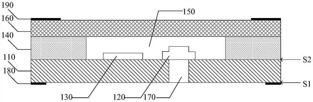
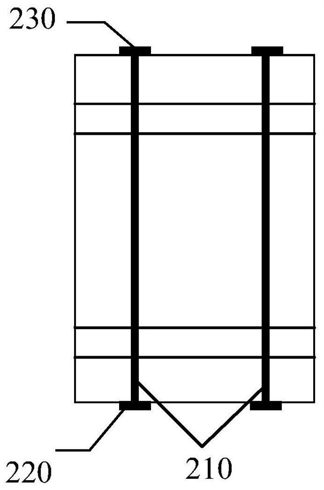
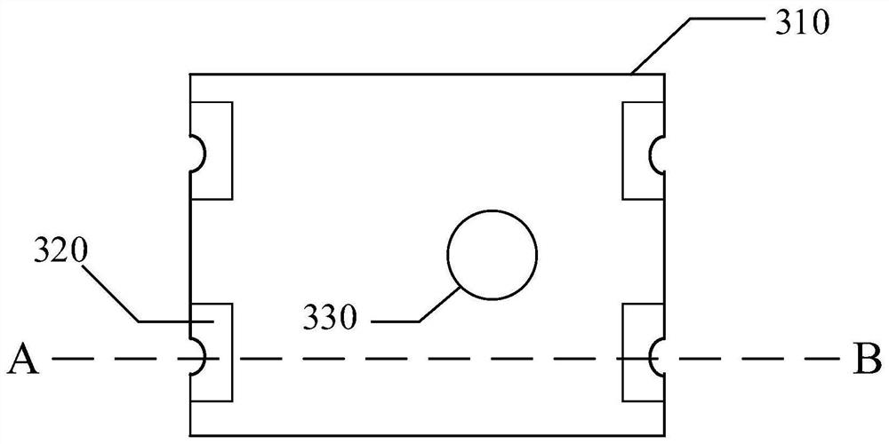
[0041] In addition, it should be noted that, for the convenience of description, only parts related to the present invention are shown in the drawings but not all content. Before discussing the exemplary embodiments in more detail, it should be mentioned that some exemplary embodiments are described as processes or methods depicted as flowcharts. Although the flowcharts describe various operations (or steps) as sequential processing, many of the operations may be performed in parallel, concurrently, or simultaneously. In addition, the order of operations can be rearranged. The process...


PUM


Abstract

The embodiment of the invention discloses a pressure module and a manufacturing method thereof. The pressure module comprises a circuit substrate, an MEMS chip, an ASIC chip, a first packaging circuitboard, a pouring sealant and a second packaging circuit board. According to the technical scheme provided by the invention, the MEMS chip and the ASIC chip are fused together and arranged in the cavity formed by the circuit substrate, the first packaging circuit board and the second packaging circuit board, and are filled with the pouring sealant, so that the purpose that the chip is sealed without leakage is achieved, the MEMS chip and the ASIC chip can be ensured not to be damaged and not to fall off at a bonding part under high pressure, and the overall structural compactness is improved;in addition, the MEMS chip and the ASIC chip are only used as pressure sensing elements, so that the reliability and the stability of a product are improved, the cost and the manufacturability and assembly cost of the pressure module are reduced, and large-scale automatic production is realized.

Description

technical field [0001] Embodiments of the present invention relate to the technical field of semiconductor chip packaging, in particular to a pressure module and a manufacturing method thereof. Background technique [0002] Micro-Electro-Mechanical Systems (MEMS for short) is a process technology that integrates microelectronics technology and mechanical engineering, and its operating range is in the micron range. MEMS is a brand-new research and development field that must consider the mixing of multiple physical fields at the same time. Compared with traditional machinery, their size is smaller, the largest is no more than one centimeter, or even only a few microns, and their thickness is even smaller. . Application Specific Integrated Circuit (ASIC for short) is considered as an integrated circuit designed for a special purpose in the integrated circuit industry. [0003] The packaging structure of MEMS chips and ASIC chips has opened up a new technical field and indust...

Claims


Application Information

Patent Timeline
IPC IPC(8): B81B7/02B81B7/00B81C1/00
CPCB81B7/0009B81B7/0041B81B7/007B81B7/02B81B2201/0264B81C1/00301B81C1/00325
Inventor 缪建民潘孝江尹长通
Owner 华景传感科技(无锡)有限公司
Why Eureka
Try Eureka