Flexible multiplication type organic photoelectric detector and preparation method

A photodetector and flexible technology, applied in photovoltaic power generation, electric solid-state devices, semiconductor/solid-state device manufacturing, etc., can solve the problem of increasing the response time of multiplier devices, and achieve the effect of enhancing electron tunneling injection and fast response speed

Inactive Publication Date: 2021-01-26
UNIV OF ELECTRONICS SCI & TECH OF CHINA
View PDF4 Cites 1 Cited by
  • Summary
  • Abstract
  • Description
  • Claims
  • Application Information

AI Technical Summary

Problems solved by technology

However, the response time of multiplied devices is greatly increased, which is determined by the principle of not utilizing the negative effects of using

Method used


Image

  • Flexible multiplication type organic photoelectric detector and preparation method
  • Flexible multiplication type organic photoelectric detector and preparation method
  • Flexible multiplication type organic photoelectric detector and preparation method

Examples


Embodiment 1

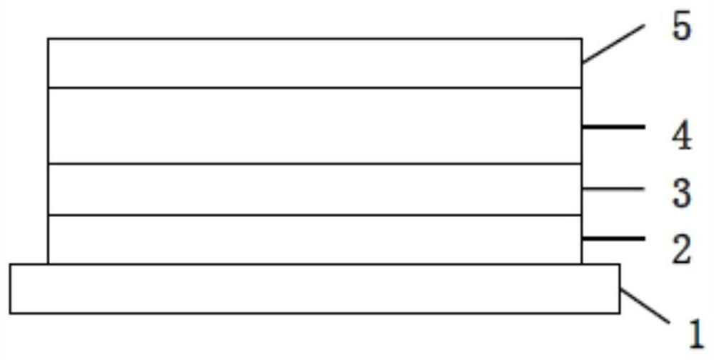
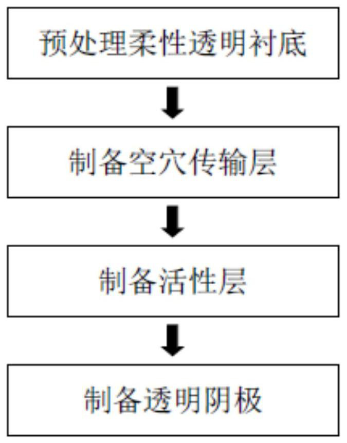
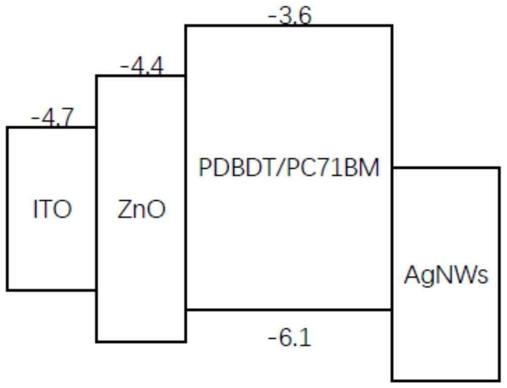
[0033] A flexible multiplication type organic photodetector provided by a preferred embodiment of the present invention includes a flexible transparent substrate layer 1, and a conductive anode layer 2, a hole transport layer 3, an active layer 4, and a conductive cathode layer are sequentially stacked on the flexible transparent substrate layer 1. 5. The active layer 4 is a mixed thin film, the thickness of the mixed thin film is 800-1200nm, and the materials for making the mixed thin film include but not limited to electron donor materials and electron acceptor materials; the electron donor materials and the electron acceptor materials The mass ratio of bulk material is 1:100~10:100. like figure 1 As shown, the flexible transparent substrate layer 1 is made of PET, the conductive anode layer 2 is ITO, the hole transport layer 3 is ZnO, the active layer 4 is a mixed film of PBDB-T and PC71BM, and the conductive cathode layer 5 is silver nanowires.

[0034] Pretreatment of fl...

Embodiment 2

[0041] The device structure diagram and fabrication flow chart described in Embodiment 2 are consistent, only one or more layers of materials or processes are replaced, and are not limited to the disclosed and described specific implementation methods.

[0042] The specific process is as follows:

[0043] 1. Pretreatment of flexible transparent substrate layer 1 with conductive anode layer 2: scrub with detergent and dust-free cloth, then rinse with deionized water to remove oil, dust, fingerprints, etc.; then use deionized water, acetone, isopropyl Alcohols were sonicated for 15 minutes, placed in a drying oven, and dried at 110°C for 60 minutes; the dried transparent substrate was irradiated with UV-ultraviolet light for 15 minutes.

[0044] 2. Prepare the hole transport layer 3 on the above-mentioned conductive anode layer 2: take 40 μL of ZnO solution, spin-coat it on the conductive anode 2 evenly at a rate of 2500 rpm for 25 s; and rapidly anneal at 150 °C in the air atmo...


PUM

PropertyMeasurementUnit
thicknessaaaaaaaaaa
thicknessaaaaaaaaaa
thicknessaaaaaaaaaa

Abstract

The invention discloses a flexible multiplication type organic photoelectric detector and a preparation method. The flexible multiplication type organic photoelectric detector comprises a flexible transparent substrate layer, a conductive anode layer, a hole transport layer, an active layer and a conductive cathode layer are sequentially stacked on the flexible transparent substrate layer, the active layer is a mixed film, the thickness of the mixed film ranges from 800 nm to 1200 nm, and materials for manufacturing the mixed film include but are not limited to an electron donor material and an electron acceptor material. The detector prepared by adopting the structure has the characteristic of high flexibility on the whole, can be applied to the field of wearable equipment, and has a practical value of miniaturization; by adjusting the mass ratio of the donor material to the acceptor material, a small amount of donor material is used as an electron trap, and electron tunneling injection is enhanced under the condition of reverse bias, so that the multiplication effect of the multiplication type device is achieved, and meanwhile, compared with a traditional multiplication type device, the detector has higher response speed.

Description

technical field [0001] The invention relates to the technical field of semiconductor photoelectric devices, in particular to a design and preparation method of a flexible multiplication type organic photodetector. Background technique [0002] Photodetector is a very important optoelectronic device, which can be widely used in military, civilian, scientific research and other fields. The core part of a digital camera that replaces a film camera - a digital image sensor, one of its important parts is a high-sensitivity photodetector. In optical communication, the whole system must at least include a sending end, a transmission medium and a receiving end, where the receiving end is a photodetector (to match with a demodulation device). Photodetectors are already indispensable basic components in the fields of social life, production, and scientific research. However, existing photodetectors still cannot meet the needs of the application field. To achieve new breakthroughs i...

Claims


Application Information

Patent Timeline
Patent Type & Authority Applications(China)
IPC IPC(8): H01L51/42H01L51/44H01L51/00H01L51/48
CPCH10K77/111H10K30/152H10K30/20H10K30/82Y02E10/549
Inventor 太惠玲巩国豪蒋亚东王洋刘青霞肖建花
Owner UNIV OF ELECTRONICS SCI & TECH OF CHINA
Why Eureka
Try Eureka