Optimization method of system-in-package structure

A system-level packaging and optimization method technology, applied in the field of microelectronics, can solve the problems of complex operation, high cost, high equipment and process requirements, etc., to avoid random errors, reduce the required time, and reduce costs.

Active Publication Date: 2021-01-29
XIDIAN UNIV
View PDF4 Cites 4 Cited by
  • Summary
  • Abstract
  • Description
  • Claims
  • Application Information

AI Technical Summary

Problems solved by technology

[0004] In recent years, research on SIP defect diagnosis and failure analysis technology has been mainly carried out at home and abroad. However, due to the complexity of SIP, higher requirements are placed on design and process technology, and its reliability is the industry's concern. Focus, and the main purpose of optimizing the SIP structure is to improve its reliability. The existing SIP reliability research mainly includes failure analysis, reliability test, process control, reliability design, etc.; but these are improved through failure analysis and process control. The reliability method has high requirements for equipment and process, so there are defects of complicated operation and high cost

Method used


Image

  • Optimization method of system-in-package structure
  • Optimization method of system-in-package structure
  • Optimization method of system-in-package structure

Examples


Embodiment Construction

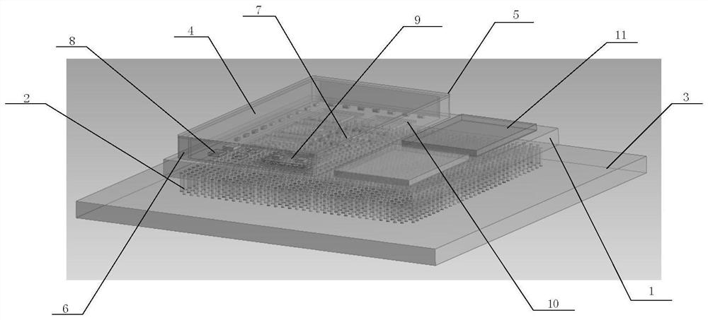
[0030] refer to figure 1 with figure 2 , The existing system-level package SIP structure is composed of low-temperature co-fired ceramic LTCC, ceramic solder column array CCGA, kovar frame, passive components, bare chips, and chip stacks. It is a low-temperature co-fired ceramic LTCC welded on the bottom surface of the ceramic welding column array CCGA. On the LTCC, passive components, bare chips, and chip stacks are assembled together, and a metal partition wall is used to construct a hermetic packaging area as a whole.

[0031] The specific SIP structure used in this example is to use low-temperature co-fired ceramics as the substrate 1, weld the ceramic welding column array 2 on the bottom surface of the substrate, and weld the other side of the ceramic welding column array with the printed circuit board 3, and the upper surface of the substrate is equipped with a Cutting frame 4 and cover plate 5, there is a gap between the boundary of the cutting frame and the substrate...


PUM


Abstract

The invention discloses an optimization method of a system-in-package SIP (Session Initiation Protocol) structure, which mainly overcomes the defects of complex operation and high cost of the existingSIP structure optimization technology, and adopts the scheme that an initial finite element model is established, and the maximum stress value A and the safety margin S of the initial finite elementmodel in a vibration state are calculated; factors influencing the stress of the SIP structure are selected; parameterizing the selected factor, and calculating the sensitivity of the factor to the SIP structure stress; selecting a high-sensitivity factor as a key factor; selecting key factor parameters to establish an orthogonal test table; according to the test table, establishing a corresponding finite element model for testing and processing to obtain a factor combination; calculating the maximum stress value and the safety margin S'under the factor combination; comparing S with S 'to obtain an optimal factor combination; and designing an SIP structure according to the optimal factor combination parameters. According to the method, the reliability of the SIP is improved in the design level, the operation complexity is reduced, the cost is reduced, and the method can be used for the structural design of system-in-package.

Description

technical field [0001] The invention belongs to the technical field of microelectronics, and in particular relates to an optimization method of a system-level packaging structure, which can be used in the structural design of a system-level packaging SIP. Background technique [0002] Today's microelectronic packaging technology is constantly improving, making the market's requirements for packaging higher and higher. Thin and short, multi-functional, low power consumption, and fast speed are the development trends of today's electronic products. The new system-in-package SIP technology continues Moore's Law at the system level, and semiconductor companies in the industry are paying more and more attention to and developing SIP. [0003] The existing SIP technology is to assemble multiple active components and passive components with different functions, multi-chip components MEMS, optical devices and other devices into a single standard package that can provide multiple fun...

Claims


Application Information

Patent Timeline
Patent Type & Authority Applications(China)
IPC IPC(8): G06F30/398G06F30/23G06F119/14
CPCG06F30/398G06F30/23G06F2119/14Y02T90/00
Inventor 董刚李依依朱思瞳朱樟明杨银堂
Owner XIDIAN UNIV
Why Eureka
Try Eureka