Semiconductor structure and forming method thereof
A technology of semiconductor and gate structure, applied in the field of semiconductor structure and its formation, can solve the problems of difficult channel and poor channel control ability of gate structure, so as to improve electrical performance, increase stress and form high quality Effect
- Summary
- Abstract
- Description
- Claims
- Application Information
AI Technical Summary
Problems solved by technology
Method used
Image

Examples
Embodiment Construction
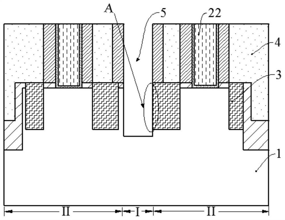
[0028] Currently formed devices still suffer from poor performance. The reasons for the poor performance of the device are analyzed in conjunction with a method of forming a semiconductor structure.
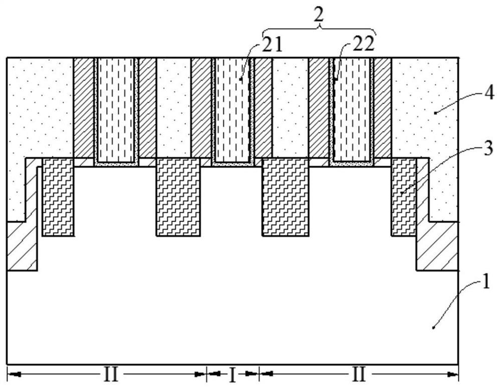
[0029] refer to figure 1 and figure 2 It is a structural schematic diagram corresponding to each step in a method for forming a semiconductor structure.
[0030] Such as figure 1 As shown, the semiconductor structure includes: a substrate, the substrate 1 includes an isolation region I and a device region II; a gate structure 2 is located on the substrate 1, and the gate structure 2 located on the isolation region I serves as A dummy gate structure 21, the gate structure 2 located on the device region II is used as a device gate structure 22; a source-drain doped region 3 is located in the substrate 1 on both sides of the gate structure 2; The interlayer dielectric layer 4 is located on the base, covers the sidewall of the gate structure 2 , and exposes the top of the gate s...
PUM
 Abstract
Description
Claims
Application Information
 - Generate Ideas
- Intellectual Property
- Life Sciences
- Materials
- Tech Scout
- Unparalleled Data Quality
- Higher Quality Content
- 60% Fewer Hallucinations
Browse by: Latest US Patents, China's latest patents, Technical Efficacy Thesaurus, Application Domain, Technology Topic, Popular Technical Reports.
© 2025 PatSnap. All rights reserved.Legal|Privacy policy|Modern Slavery Act Transparency Statement|Sitemap|About US| Contact US: help@patsnap.com