Chip signal testing device and method based on solder ball array packaging

A technology of solder ball array packaging and signal testing, which is applied in the direction of measuring devices, measuring device shells, and electronic circuit testing, etc., can solve the problems of signal distortion, error, and inductive or capacitive load errors without considering the lead impedance matching relationship, etc. To achieve the effect of improving reliability and avoiding noise coupling

Pending Publication Date: 2021-02-09
CSR ZHUZHOU ELECTRIC LOCOMOTIVE RES INST
View PDF0 Cites 0 Cited by
  • Summary
  • Abstract
  • Description
  • Claims
  • Application Information

AI Technical Summary

Problems solved by technology

The general test fixture simply leads the high-speed signal through the test cable to facilitate detection, but does not consider the impedance matching relationship between the lead wire and the actual signal line and the error of the inductive or capacitive load due to welding problems. Further distortion of the signal will also introduce errors to interfere with the reliable operation of the system, and the test will get wrong results

Method used


Image

  • Chip signal testing device and method based on solder ball array packaging
  • Chip signal testing device and method based on solder ball array packaging
  • Chip signal testing device and method based on solder ball array packaging

Examples


Embodiment Construction

[0030] The present invention will be further described below in conjunction with the accompanying drawings and specific embodiments.

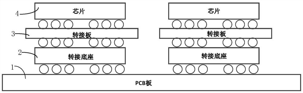
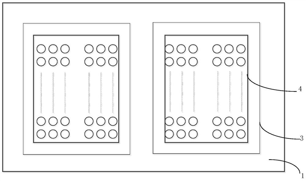
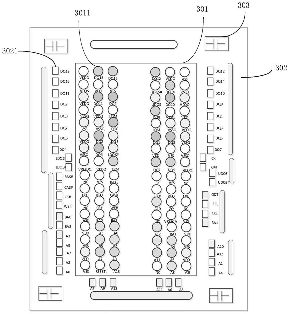
[0031] Such as Figure 1 to Figure 4 As shown, the chip signal testing device based on solder ball array packaging in this embodiment includes an adapter base 2, an adapter board 3, an active probe 5 and an oscilloscope 6; the bottom side of the adapter base 2 and the PCB board where the chip 4 is located The pads of 1 are connected correspondingly to raise the pads of PCB 1; the bottom side of the adapter board 3 and the top side of the adapter base 2 are connected by solder balls, and the top side of the adapter board 3 is provided with pads. The pads of the adapter board 3 include a connection terminal 3011 for connecting with the chip 4 to be tested through solder balls and a test terminal 3021 connected to the connection terminal 3011 , and the test terminal 3021 is connected to the oscilloscope 6 through the active probe 5 .

[0032] In ...


PUM


Abstract

The invention discloses a chip signal testing device based on solder ball array packaging. The chip signal testing device comprises an adapter base, an adapter plate, an active probe and an oscilloscope, the bottom side of the adapter base is correspondingly connected with a bonding pad of a PCB where a chip is located and is used for lifting the bonding pad of the PCB. The bottom side of the adapter plate is connected with the top side of the adapter base through a solder ball, the bonding pad is arranged on the top side of the adapter plate, the bonding pad of the adapter plate comprises a connecting end used for being connected with a chip to be tested through the solder ball and a testing end connected with the connecting end, and the testing end is connected with the oscilloscope through the active probe. The invention also discloses a testing method. The testing method comprises the following steps: S01, extracting S parameters of a measurement channel where each test end of theadapter plate is located in advance; and S02, when the signal of the chip is measured, de-embedding the measurement channel according to the S parameters of the measurement channel to obtain a de-embedded waveform. The testing device and method have the advantages of being accurate and reliable in testing and the like.

Description

technical field [0001] The invention mainly relates to the technical field of chip signal testing, in particular to a chip signal testing device and testing method based on solder ball array packaging. Background technique [0002] As the chip pins of the integrated circuit increase, its power consumption also increases, and the chip using the BGA package (ball array package) can effectively reduce the volume and increase the heat dissipation performance, and the ensuing problem is high There are problems in IC signal detection and conformance testing of dense BGA packages. Generally, testable points are reserved in the hardware design stage. However, due to signal integrity and other issues, the signal at the testable points and BGA solder balls is Due to the capacitive load characteristics at the test point, the signal waveform quality is distorted, and there may be hook or ringing. Therefore, the most realistic signal waveform data can be obtained only by testing the sol...

Claims


Application Information

Patent Timeline
IPC IPC(8): G01R31/28G01R1/04
CPCG01R31/2896G01R31/2886G01R31/2891
Inventor 汪旭李明刘海洋王磊曾雄邓洲洋易君谓李法俊
Owner CSR ZHUZHOU ELECTRIC LOCOMOTIVE RES INST
Why Eureka
Try Eureka