Universal alternate sampling ADC system

A technology of acquisition circuit and clock management, applied in the field of electronics, can solve the problems affecting the versatility and design cycle and difficulty of alternate sampling ADC, ADC output spectrum spurious, and difficulty in PCB layout design, so as to improve chip versatility and resistance to resistance. Interference ability, optimizing timing mismatch and bandwidth mismatch, reducing the effect of thermal design difficulty

Pending Publication Date: 2021-02-19
CHINA SOUTH IND GRP AUTOMATION RES INST
View PDF3 Cites 0 Cited by
  • Summary
  • Abstract
  • Description
  • Claims
  • Application Information

AI Technical Summary

Problems solved by technology

In the existing alternate sampling technology, there are four kinds of mismatch problems among the ADCs: offset mismatch, gain mismatch, timing mismatch and bandwidth mismatch, resulting in spurs in the ADC output spectrum and overall performance degradation
The above four kinds of mismatch problems mainly come from the design and production of the chip itself and the circuit and PCB, which means that in order to ensure the performance, the alternate sampling ADC system needs to be redesigned and debugged in different circuits, which greatly affects the versatility of the alternate sampling ADC. and design cycle and difficulty
At present, the alternate sampling ADC mostly uses the differential LVDS interface as the data interface, the number of pins is large, and the device package is large; the requirements for equal-length traces are strict, and the PCB layout design is difficult, which makes it difficult to directly transplant the alternate sampling system to other circuits.
Even if it is hoped to use system-in-package technology (SIP) to package the alternate sampling ADC system circuit into a chip, the numerous pins and traces of the LVDS parallel data interface will greatly increase the packaging cost and difficulty, which also limits the alternate sampling ADC system in different applications. circuit use
In practical applications, the requirements for ADC sampling rate and bandwidth are getting higher and higher, resulting in faster and faster ADC data interface rate. Traditional parallel transmission interfaces such as LVDS and CMOS can no longer fully meet the requirements of high-speed sampling in terms of data interface rate.

Method used


Image

  • Universal alternate sampling ADC system
  • Universal alternate sampling ADC system

Examples


Embodiment 1

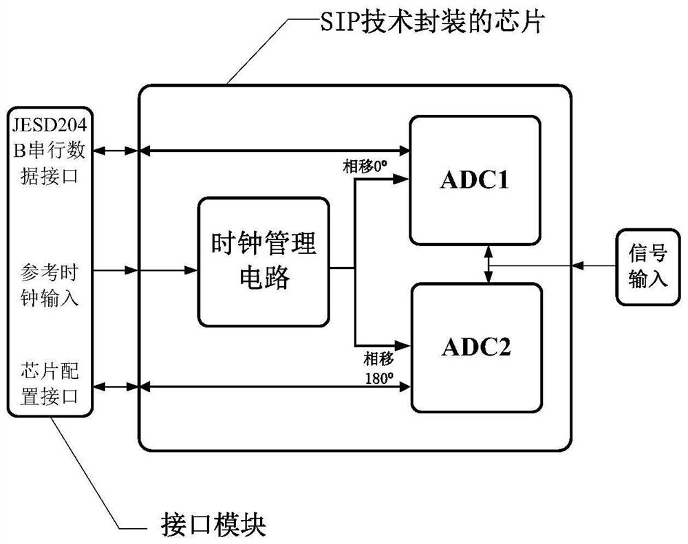
[0028] In the existing alternate sampling technology, there are four kinds of mismatch problems among the ADCs: offset mismatch, gain mismatch, timing mismatch and bandwidth mismatch, which lead to spurs in the ADC output spectrum and a decrease in the overall performance of the system. The existing technology In order to ensure the system performance, the alternate sampling ADC system needs to be redesigned and debugged in different circuits, which greatly affects the versatility, design cycle and difficulty of the alternate sampling ADC.

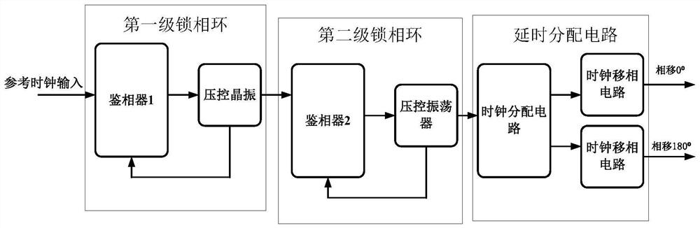
[0029] Therefore, if figure 1 As shown, a kind of general alternate sampling ADC system of the present invention comprises an ADC acquisition circuit composed of an interface module, a clock management circuit, and several independently working ADCs, and the interface module is composed of a data interface, a reference clock input, and a chip configuration interface, and is characterized in that , the ADC acquisition circuit is communicati...


PUM


Abstract

The invention discloses a universal alternate sampling ADC system. A JESD204B serial data interface is used as a data interface; mismatch and gain mismatch between the ADCs are matched in a calibration mode; a clock management circuit is adjusted for clock phases among the ADCs to optimize time sequence mismatch and bandwidth mismatch; and the optimized clock management circuit and the calibratedADC acquisition circuit are integrated and packaged into a chip by adopting a system packaging technology (SIP). According to the system, the design period and difficulty of the alternate sampling ADCsystem caused by four mismatch problems of mismatch, gain mismatch, time sequence mismatch and bandwidth mismatch are solved, and the universality and anti-interference performance of the alternate sampling ADC system are improved.

Description

technical field [0001] The invention relates to electronic technology, in particular to a general alternate sampling ADC system. Background technique [0002] Alternate sampling ADC refers to two or more ADCs with a defined clock relationship synchronously sampling input signals and combining them to generate output signals. It is generally used in the acquisition of high-speed broadband signals. The combination of multiple low-sampling rate ADCs is used to increase the sampling rate. and bandwidth. In the existing alternate sampling technology, there are four kinds of mismatch problems among the ADCs: offset mismatch, gain mismatch, timing mismatch and bandwidth mismatch, resulting in spurious output spectrum of the ADC and overall performance degradation. The above four kinds of mismatch problems mainly come from the design and production of the chip itself and the circuit and PCB, which means that in order to ensure the performance, the alternate sampling ADC system need...

Claims


Application Information

Patent Timeline
Patent Type & Authority Applications(China)
IPC IPC(8): H03M1/34
CPCH03M1/34
Inventor 陈羲聪周凯李宸极
Owner CHINA SOUTH IND GRP AUTOMATION RES INST
Why Eureka
Try Eureka