A wire etching method for gold-plated printed circuit boards

A circuit board and wire technology, which is applied in the field of wire etching of gold-plated circuit boards, can solve the problems of discoloration, high cost, quality defects, etc.

Active Publication Date: 2022-04-29
珠海杰赛科技有限公司 +1
View PDF13 Cites 0 Cited by
  • Summary
  • Abstract
  • Description
  • Claims
  • Application Information

AI Technical Summary

Problems solved by technology

However, on the one hand, the wet film cover wire method will cause discoloration when used on PTFE+ceramic plates, and on the other hand, the production process is long, resulting in high costs. The combination of the dry film and the circuit is not good, the potion will penetrate through the gap, and the wire will be plated with nickel and gold to cause permeation, which cannot be removed during etching and leads to residual wires, resulting in quality defects

Method used


Image

  • A wire etching method for gold-plated printed circuit boards

Examples


Embodiment Construction

[0019] In order to make the object, technical solution and advantages of the present invention clearer, the present invention will be further described in detail below in conjunction with the accompanying drawings and embodiments. It should be understood that the specific embodiments described here are only used to explain the present invention, not to limit the present invention.

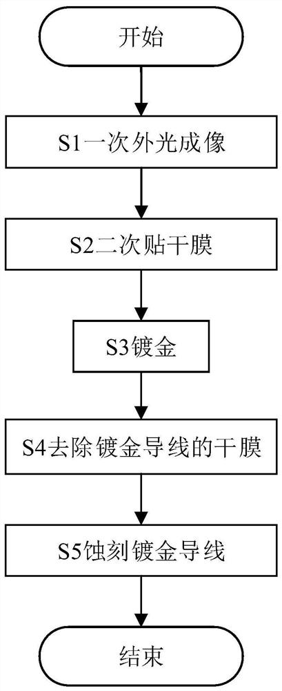
[0020] see figure 1 , the wire etching method for gold-plated circuit board of the present embodiment comprises:

[0021] Step S1, an external light imaging, a dry film is applied on the surface of the circuit board, and then the protective film is torn off, and the imaging of the gold-plated wire and the gold-plated area is performed. The equipment used for imaging is an LDI exposure machine;

[0022] Step S2, apply the dry film for the second time, and perform secondary external light imaging after the dry film is applied to the circuit board to expose the gold-plated area. To protect the gold-...


PUM

PropertyMeasurementUnit
thicknessaaaaaaaaaa
thicknessaaaaaaaaaa

Abstract

The wire etching method for a gold-plated circuit board provided by the present invention includes S1, primary external light imaging; S2, secondary dry film application, performing secondary external light imaging after secondary dry film application on the circuit board to expose the gold-plated area, The temperature of the film is 110°C-120°C, and the pressure of the film is 0.4-0.6MPa; S3, gold-plated; S4, remove the dry film of the gold-plated wire; S5, etch the gold-plated wire. It can be seen from the above scheme that the dry film is pasted twice to provide sufficient glue to fill the line gap and avoid gaps at the edge of the line. The film is reliably attached to the circuit board, avoids seepage, can completely etch the wire, solves the problem of wire residue, avoids electrical performance problems caused by the wire residue on the circuit board, and improves the reliability of the circuit board.

Description

technical field [0001] The invention belongs to the technical field of circuit boards, in particular to a wire etching method for gold-plated circuit boards. Background technique [0002] Circuit board, also known as PCB, printed circuit board, which uses insulating board as the base material, cuts to a certain size, has at least one conductive pattern on it, and is equipped with holes (such as component holes, fastening holes, metallized holes, etc.) ), used to replace the chassis of the previous installation of electronic components and realize the interconnection between electronic components. [0003] Most of the existing circuit boards used in aerospace products require thick gold plating, and the thickness of gold is not less than 2.5 μm, especially the top surface of the pad, and the four sides of any three sides of the top, bottom, left, and right sides are required to be covered with gold. The multi-pattern is an isolated pad, and no via holes and conductive lines ...

Claims


Application Information

Patent Timeline
Patent Type & Authority Patents(China)
IPC IPC(8): H05K3/00H05K3/18
CPCH05K3/0082H05K3/188H05K2203/056
Inventor 何家添吉祥书关志峰
Owner 珠海杰赛科技有限公司
Why Eureka
Try Eureka