Reduction of black silicon in semiconductor manufacture

A semiconductor and black silicon technology, applied in the field of reducing the formation of black silicon, can solve problems such as affecting the resolution or reliability and corrosion uniformity of lithography, and reducing the yield of chips

Inactive Publication Date: 2003-10-08
SIEMENS AG +1
View PDF5 Cites 0 Cited by
  • Summary
  • Abstract
  • Description
  • Claims
  • Application Information

AI Technical Summary

Problems solved by technology

However, the use of clamp rings creates finger shielding, which can affect lithograph

Method used


Image

  • Reduction of black silicon in semiconductor manufacture
  • Reduction of black silicon in semiconductor manufacture
  • Reduction of black silicon in semiconductor manufacture

Examples


Embodiment Construction

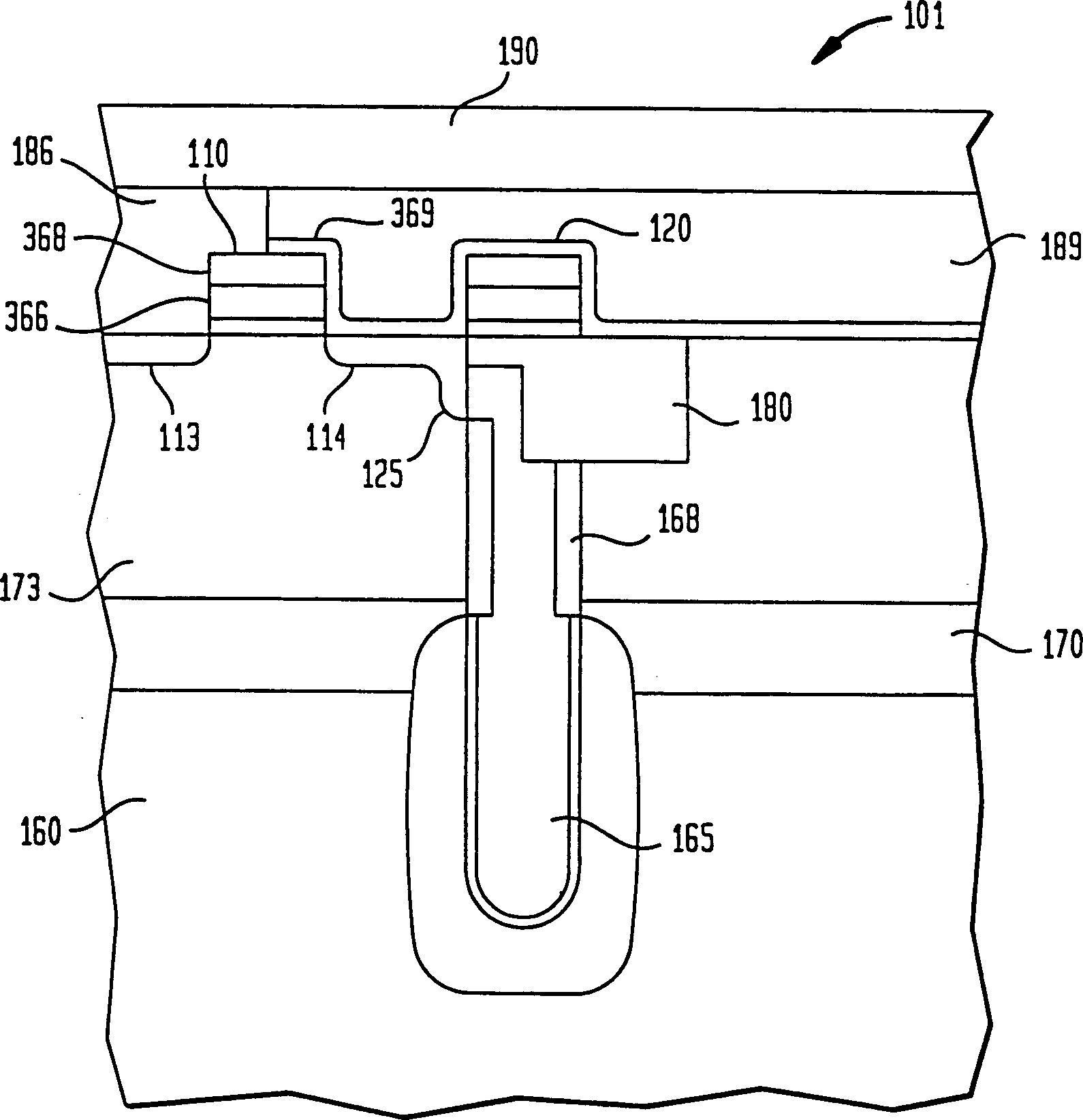
[0020] The present invention relates to preventing the formation of black silicon during the manufacture of integrated circuits (ICs). ICs, for example, include memory circuits such as random access memories (RAMs), dynamic RAMs (DRAMs), synchronous DRAMs (SDRAMs), static RAMs (SRAMs), or read only memories (ROMs). Furthermore, ICs may also include logic devices such as programmable logic arrays (PLAs), application specific ICs (ASICs), merged DRAM-logic ICs (embedded DRAMs), or any other circuit devices.

[0021] Typically, many parallel ICs are fabricated on a substrate such as a silicon wafer. After processing, the wafer is diced in order to separate the ICs into individual chips. The chips are then packaged into final products that are used, for example, in consumer products such as computer systems, cellular telephones, personal digital assistant devices (PADs) and other products.

[0022] For purposes of discussion, a conventional DRAM cell will first be described. re...


PUM


Abstract

Reduction of black silicon is achieved by providing a protective device layer in the bead region and sides of the wafer before the formation of a hard etch mask.

Description

technical field [0001] The present invention relates generally to semiconductor manufacturing, and more particularly to reducing the formation of black silicon. Background technique [0002] In the manufacture of integrated circuits (ICs) or chips, vias or trenches are typically formed in substrates such as silicon wafers for various purposes. Vias or trenches are formed by etching into the substrate. Deep trenches (DTs), for example, function as trench capacitors for memory cell arrays. [0003] Typically, DTs are formed by first providing a substrate stack on the wafer surface. The base stack includes, for example, successive layers of base oxide 112 and base nitride 114 . On top of the substrate stack is a hard mask layer 116 comprising, for example, TEOS. The hard mask layer functions as a hard etch mask for forming DTs. [0004] A photoresist layer is deposited on the hard mask layer and patterned to selectively expose areas where DTs are to be formed. Typically, ...

Claims


Application Information

Patent Timeline
IPC IPC(8): H01L21/302H01L21/3065H01L21/308H01L21/8242H01L27/108
CPCH01L21/3083H01L21/70
Inventor 王廷浩彭登青D·M·多布岑斯凯R·S·维瑟
Owner SIEMENS AG
Why Eureka
Try Eureka