Check patentability & draft patents in minutes with Patsnap Eureka AI!

Substrate defect inspection device and method

A defect inspection and substrate technology, which is applied in the field of defect devices, can solve the problems of PCB manufacturing yield reduction, emotional errors, and identification of unqualified PCBs, and achieve the effect of improving yield and maintaining consistency

Pending Publication Date: 2021-02-23
LAONPEOPLE
View PDF0 Cites 0 Cited by
  • Summary
  • Abstract
  • Description
  • Claims
  • Application Information

AI Technical Summary

Problems solved by technology

Therefore, there is a problem that in order to prevent such a situation, it is necessary to additionally use other equipment to inspect the PCB and identify whether the state of the PCB is acceptable or unacceptable
[0005] In addition, there is also a problem that since it is impossible for every operator who inspects PCBs to maintain a constant level of inspection standards, emotional errors, etc., will occur, which will reduce the consistency of product inspection results, thereby reducing the yield rate of manufactured PCBs. reduce

Method used


Image

  • Substrate defect inspection device and method
  • Substrate defect inspection device and method
  • Substrate defect inspection device and method

Examples


Embodiment Construction

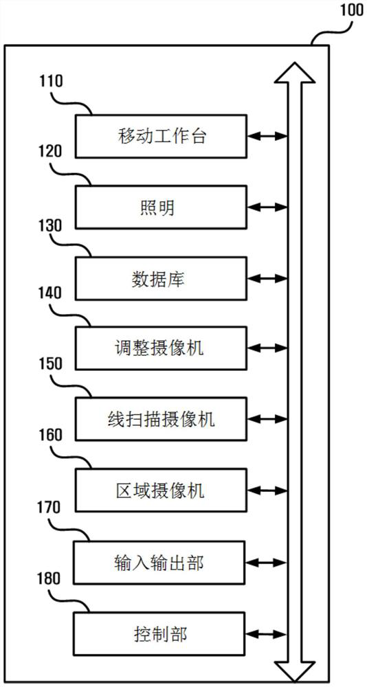
[0034] Hereinafter, each embodiment will be described in detail with reference to the drawings. The embodiments described below can be modified and implemented in various forms. In order to more clearly describe the features of each embodiment, detailed descriptions of matters known to those of ordinary skill in the art to which each embodiment pertains below are omitted. In addition, in the drawings, parts irrelevant to the description of the respective embodiments are omitted, and similar reference numerals are assigned to similar parts throughout the specification.

[0035] Throughout the specification, when a certain structure is "connected" to another structure, this includes not only the case of "directly connected" but also the case of "connected with other structures interposed therebetween". In addition, when a certain structure "includes" a certain structure, unless otherwise specified, it means that other structures may also be included rather than excluding other ...


PUM


Abstract

A substrate defect inspection device of the present invention comprises: a moving table for moving a substrate to an inspection position; an illumination unit that illuminates the substrate with a predetermined light in order to acquire a captured image; at least one line scanning camera that captures an image of the substrate in units of predetermined lines; at least one region camera that captures an image of the substrate in units of predetermined regions; a database storing images for detecting defects of the substrate; and a control unit for detecting a primary defect by moving the position of the substrate with the moving table, controlling illumination to acquire, by the line scanning camera, an image obtained by imaging a plating layer portion of the substrate and an image obtainedby imaging a solder resist layer portion, and determining, on the basis of the acquired images, the state of the substrate as one of normality, defect, and re-inspection, and for detecting a re-defect by controlling illumination of the substrate determined to be re-inspected, acquiring a substrate image in which the substrate is imaged by the region camera, and determining the state of the substrate to be normal or defective on the basis of the acquired substrate image.

Description

technical field [0001] Embodiments disclosed in this specification relate to an apparatus and method for inspecting defects of a substrate. More specifically, it relates to a substrate defect inspection device and method that do not require reconfirmation of defects on substrates such as printed circuit boards. Background technique [0002] Since various types of defects may occur, various types of inspections are performed on products such as printed circuit boards (PCB: Printed Circuit Board) for shipment. For example, in the prior art document related to this, Korean Laid-Open Patent No. 10-2005-0103525, a PCB inspection and screening device is described, which is used to prevent the circuit patterns and probes formed on the lower surface of the PCB before leaving the factory. Checks are made on the basis of excessive contact between them. [0003] In order to inspect printed circuit boards, rule base inspections are performed in addition to electrical inspections as in...

Claims


Application Information

Patent Timeline
Patent Type & Authority Applications(China)
IPC IPC(8): G01N21/956
CPCG01N21/956G01N2021/95638G01N21/8806G01N21/9501G01N21/8851G06T7/0004G01B11/30G01N2021/8887
Inventor 李在旻宋德王朴昌成
Owner LAONPEOPLE
Features
  • R&D
  • Intellectual Property
  • Life Sciences
  • Materials
  • Tech Scout
  • Unparalleled Data Quality
  • Higher Quality Content
  • 60% Fewer Hallucinations
Learn More