Check patentability & draft patents in minutes with Patsnap Eureka AI!

OLED display panel and preparation method thereof

A display panel and substrate substrate technology, which is applied in semiconductor/solid-state device manufacturing, electrical components, diodes, etc., can solve problems such as difficulty, rising production costs, and complicated processes, and achieve the effect of increasing the aperture ratio and saving electrode technology

Pending Publication Date: 2021-02-26
SHENZHEN CHINA STAR OPTOELECTRONICS SEMICON DISPLAY TECH CO LTD
View PDF6 Cites 2 Cited by
  • Summary
  • Abstract
  • Description
  • Claims
  • Application Information

AI Technical Summary

Problems solved by technology

[0004] An embodiment of the present invention provides an OLED display panel, which is used to solve the technical problems that the OLED display panel of the prior art is provided with a transparent capacitor, which leads to an increase in production cost, and the process is complicated and difficult.

Method used


Image

  • OLED display panel and preparation method thereof
  • OLED display panel and preparation method thereof
  • OLED display panel and preparation method thereof

Examples


Embodiment Construction

[0020] The following will clearly and completely describe the technical solutions in the embodiments of the present invention with reference to the drawings in the embodiments of the present invention. In the drawings, for clarity and ease of understanding and description, the size and thickness of the components shown in the drawings are not in scale.

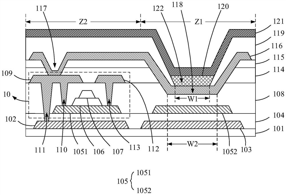
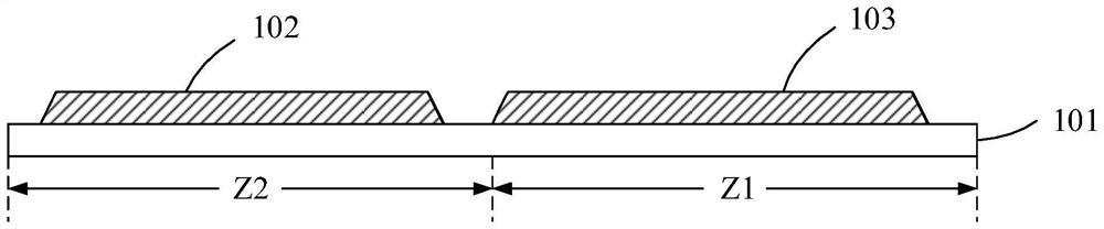
[0021] Such as figure 1 As shown, in the schematic cross-sectional view of the basic structure of the OLED display panel provided by the embodiment of the present invention, the OLED display panel defines a plurality of array-arranged pixel regions ( figure 1 Only one pixel area is shown in the figure), each pixel area is divided into a light-emitting area Z1 and a non-light-emitting area Z2, and the OLED display panel includes: a base substrate 101, a light-shielding metal layer 102, and a color filter layer 103 , the TFT structure layer 10 , the first transparent electrode layer 1052 , and the pixel electrode layer 116 . T...


PUM

PropertyMeasurementUnit
thicknessaaaaaaaaaa
thicknessaaaaaaaaaa
thicknessaaaaaaaaaa

Abstract

The invention provides an OLED display panel and a preparation method thereof. The OLED display panel comprises: an underlay substrate; a shading metal layer located on the underlay substrate and corresponding to a non-light-emitting area; a color filter layer located on the underlay substrate and corresponding to a light-emitting area; a TFT structure layer located on the side, away from the underlay substrate, of the shading metal layer; a first transparent electrode layer located on the side, away from the underlay substrate, of the color filter layer; and a pixel electrode layer located onthe TFT structure layer and the first transparent electrode layer. The first transparent electrode layer and the active layer of the TFT structure layer are arranged on the same layer. A coupling capacitor is formed in the light-emitting area and between the pixel electrode layer and the first transparent electrode layer. According to the invention, while the active layer is formed, a layer of atransparent electrode is formed in the light-emitting area and forms the coupling capacitor with the pixel electrode layer at the top, so one electrode process can be saved.

Description

technical field [0001] The invention relates to the field of display technology, in particular to an OLED display panel and a preparation method thereof. Background technique [0002] AMOLED display panels are the development trend of the panel industry. Compared with liquid crystal display panels, OLED display panels have the advantages of simple structure, wider color gamut, and faster response time. AMOLED display panels are currently mass-produced as bottom-emitting OLED display panels. [0003] In the prior art bottom-emitting OLED display panel, by adding a layer of electrode in the light-emitting area on the base substrate as the first plate of the transparent capacitor, while forming the active layer, a layer of oxide oxide is formed in the light-emitting area at the same time. The material semiconductor layer is used as the second plate of the transparent capacitor, that is, the capacitor area and the light emitting area are combined to increase the aperture ratio ...

Claims


Application Information

Patent Timeline
Patent Type & Authority Applications(China)
IPC IPC(8): H01L27/32H01L51/52H01L21/77
CPCH10K59/38H10K59/131H10K50/805H10K59/1201
Inventor 马倩周星宇
Owner SHENZHEN CHINA STAR OPTOELECTRONICS SEMICON DISPLAY TECH CO LTD
Features
  • R&D
  • Intellectual Property
  • Life Sciences
  • Materials
  • Tech Scout
  • Unparalleled Data Quality
  • Higher Quality Content
  • 60% Fewer Hallucinations
Learn More