
Semiconductor device package assembly and manufacturing method thereof

A device package and semiconductor technology, applied in semiconductor/solid-state device manufacturing, semiconductor devices, semiconductor/solid-state device components, etc., can solve semiconductor device damage, reduce device and/or system reliability, shorten devices or related The operating life of components and other issues

Pending Publication Date: 2021-03-05
SEMICON COMPONENTS IND LLC
View PDF0 Cites 0 Cited by
  • Summary
  • Abstract
  • Description
  • Claims
  • Application Information

AI Technical Summary

Problems solved by technology

Such increased thermal resistance can lead to excessive heating of the semiconductor device (e.g., a power semiconductor device), which can cause damage to the semiconductor device (or other components in a system including the semiconductor device), and / or can shorten the device or associated operating life of the components (e.g., reduced device and / or system reliability)
Furthermore, use of such TIMs can increase manufacturing and / or product costs due at least to material costs and processing operations associated with coupling the TIMs to the associated semiconductor device package and external heat transfer mechanism

Method used


Image

  • Semiconductor device package assembly and manufacturing method thereof
  • Semiconductor device package assembly and manufacturing method thereof
  • Semiconductor device package assembly and manufacturing method thereof

Examples


Embodiment Construction

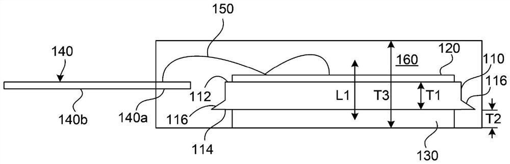
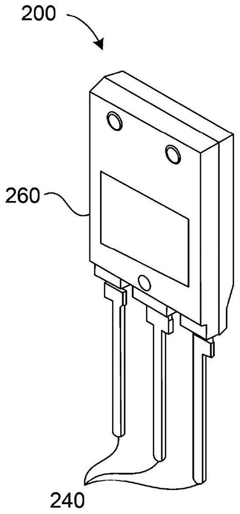
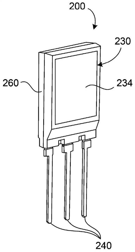
[0014] A semiconductor device assembly (e.g., semiconductor device package, packaged semiconductor device, packaged device, etc.), such as those described herein, may include a die attach paddle, one or more semiconductor die (e.g., disposed on die attach paddle), one or more signal leads, one or more wire bonds that electrically couple the one or more semiconductor dies and / or the one or more signal leads to each other, and isolation substrate. Exemplary implementations described herein may overcome at least some of the disadvantages discussed above. For example, in some implementations, the isolation substrate can include a ceramic substrate that separates an external heat dissipation surface (eg, a metal layer disposed on the ceramic substrate) from one or more semiconductor die, die-attached Connect to the blades and other electrical isolation. Additionally, the use of an isolating substrate, such as in the exemplary implementations described herein, may allow for the el...


PUM

PropertyMeasurementUnit
Thicknessaaaaaaaaaa

Abstract

The invention relates to a semiconductor device package assembly and a method of manufacturing the same. In one general aspect, a semiconductor device package can include a die attach paddle having afirst surface and a second surface that is opposite the first surface. The package can also include a semiconductor die coupled with the first surface of the die attach paddle. The package can furtherinclude a direct-bonded-metal (DBM) substrate. The DBM substrate can include a ceramic layer having a first surface and a second surface that is opposite the first surface; a first metal layer disposed on the first surface of the ceramic layer and coupled with the second surface of the die attach paddle; and a second metal layer disposed on the second surface of the ceramic layer. The second metal layer can be exposed external to the semiconductor device package. The second metal layer can be electrically isolated from the first metal layer by the ceramic layer.

Description

technical field [0001] The present invention relates generally to semiconductor device packages, such as semiconductor device packages having electrically isolated external heat dissipation surfaces, and associated methods of manufacture. Background technique [0002] Embodiments of the semiconductor device package may include externally exposed surfaces (eg, metal surfaces) for dissipating heat generated by operation of the associated semiconductor device(s), wherein the external heat dissipation The surface is electrically connected (directly or indirectly) to the semiconductor device (die) and / or to the semiconductor device included in the package, such as through the surface of the die, die attach paddles, metal heat slugs, and the like. In such implementations, external heat transfer mechanisms (e.g., heat sinks, heat pipes, etc.) (in conjunction with heat dissipation surfaces of the package) may also be used to dissipate heat generated by the semiconductor device durin...

Claims


Application Information

Patent Timeline
IPC IPC(8): H01L23/15H01L23/31H01L23/367H01L21/50H01L21/56
CPCH01L23/15H01L23/3114H01L23/3121H01L23/367H01L21/50H01L21/56H01L23/49562H01L23/49524H01L23/49568H01L23/4334H01L23/3735H01L23/3107H01L23/3142H01L2224/4903H01L2224/48247H01L2224/73265H01L2924/181H01L2224/49111H01L2224/0603H01L2224/48139H01L2224/8385H01L2224/83801H01L2224/2929H01L2224/29101H01L24/29H01L24/83H01L2924/00014H01L24/32H01L24/48H01L24/73H01L24/49H01L2924/18301H01L2924/00012H01L2924/0665H01L2924/014H01L2224/32245H01L2224/45099H01L23/49811H01L2224/80895H01L23/49506H01L23/49861
Inventor 林承園金正大全五燮
Owner SEMICON COMPONENTS IND LLC
Learn More