Packaging structure of millimeter wave antenna module and mobile equipment

A millimeter-wave antenna and packaging structure technology, applied in antenna grounding switch structure connection, antenna support/mounting device, antenna, etc., can solve the problem of millimeter-wave module section thickness, etc., to reduce section thickness, improve isolation, Effect of reducing module thickness

Pending Publication Date: 2021-03-12
SHENZHEN SUNWAY COMM
View PDF0 Cites 0 Cited by
  • Summary
  • Abstract
  • Description
  • Claims
  • Application Information

AI Technical Summary

Problems solved by technology

However, due to the larger BGA solder balls, the profile of the mmWave module is thicker
And because the mobile device is relatively thin, it is difficult to put it directly into a terminal such as a mobile phone

Method used


Image

  • Packaging structure of millimeter wave antenna module and mobile equipment
  • Packaging structure of millimeter wave antenna module and mobile equipment

Examples


Embodiment 1

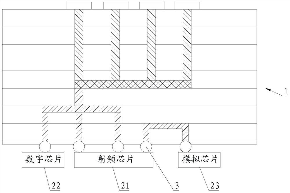
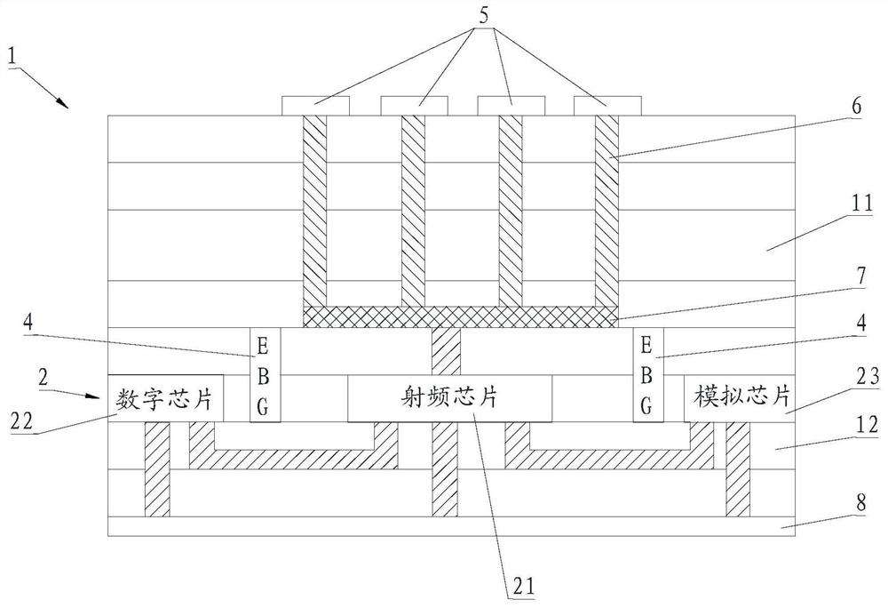
[0027] Please refer to figure 2 , Embodiment 1 of the present invention is: a packaging structure of a millimeter-wave antenna module, which is applicable to the scene of multiple chips of a millimeter-wave module in a 5G millimeter-wave communication system.

[0028] like figure 2 As shown, it includes a multilayer circuit board 1 and a chip 2, the multilayer circuit board 1 includes a first circuit board layer 11 and a second circuit board layer 12 stacked, and the chip 2 is arranged on the first circuit board Between the layer 11 and the second circuit board layer 12; the number of chips 2 is more than two, and an electromagnetic band gap 4 is set between two adjacent chips 2 .

[0029] Among them, the multilayer board is a multilayer wiring layer, and there is a dielectric layer between every two layers. A multilayer circuit board has at least three conductive layers, two of which are on the outer surface, while the remaining layer is synthesized inside the insulating ...


PUM


Abstract

The invention discloses a millimeter wave antenna module packaging structure and a mobile device. The packaging structure comprises a multilayer circuit board and a chip; the multilayer circuit boardcomprises a first circuit board layer and a second circuit board layer which are arranged in a stacked manner, and the chip is arranged between the first circuit board layer and the second circuit board layer; the number of the chips is greater than two, and an electromagnetic band gap is arranged between two adjacent chips. According to the invention, the thickness of the section of the millimeter wave module can be reduced, and the isolation between chips can be improved.

Description

technical field [0001] The invention relates to the technical field of antenna module packaging, in particular to a packaging structure of a millimeter wave antenna module and a mobile device. Background technique [0002] With the improvement of integrated circuit technology level, monolithic microwave integrated circuits are more and more widely used, especially the popularization of 5G millimeter wave, hand-held mobile terminals and base stations are widely used in millimeter wave power amplifiers, low noise amplifiers, direction shifters and RF chips such as mixers, in addition to power management (analog chips), digital chips such as FPGAs and single-chip microcomputers used for electromagnetic beam control. For the stable operation of various chips without interfering with each other, improving chip isolation is a problem to be solved. [0003] At the same time, for mobile 5G mmWave modules, the industry chooses to use the combination of RF chips and substrate antenna...

Claims


Application Information

Patent Timeline
Patent Type & Authority Applications(China)
IPC IPC(8): H01L23/66H01L23/552H01L25/18H01Q1/22H01Q1/38H01Q1/50
CPCH01L23/552H01L23/66H01L25/18H01L2223/6677H01Q1/2283H01Q1/38H01Q1/50
Inventor 赵伟侯张聚唐小兰戴令亮谢昱乾
Owner SHENZHEN SUNWAY COMM
Why Eureka
Try Eureka