Wafer fixing ring as well as preparation method and application thereof
A wafer fixing and spraying technology, applied in metal material coating process, vacuum evaporation plating, coating and other directions, can solve the problems of time-consuming and laborious assembly process, complex structure, etc., and achieve the effect of avoiding adverse effects
- Summary
- Abstract
- Description
- Claims
- Application Information
AI Technical Summary
Problems solved by technology
Method used
Image

Examples
Embodiment 1
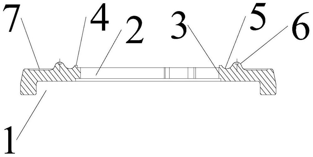
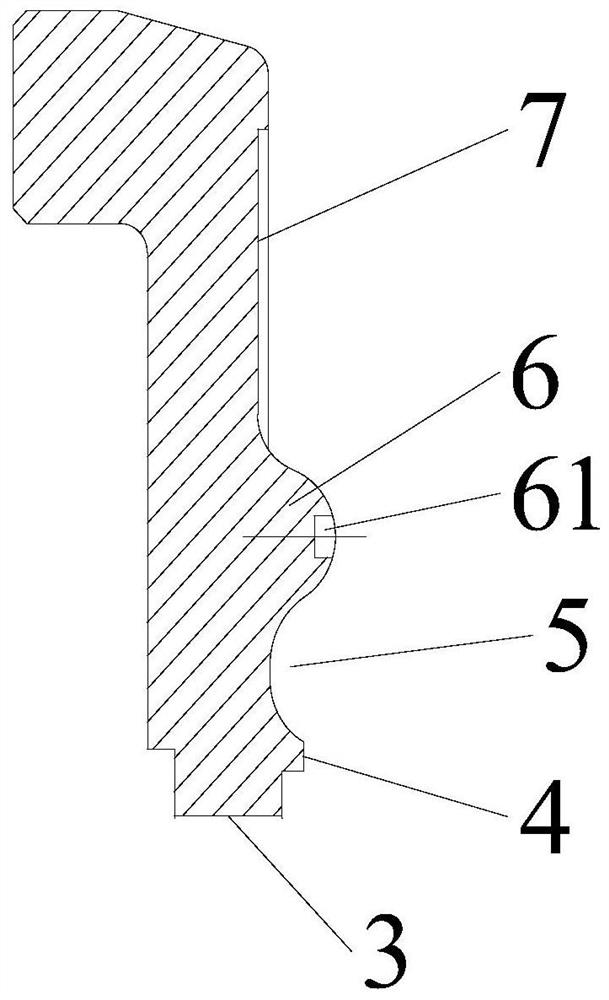
[0067] This embodiment provides a method for preparing a wafer fixing ring, the cross-sectional view of the wafer fixing ring is as follows figure 1 As shown, the partial enlarged view of the cross-sectional view is shown in figure 2 As shown, the wafer fixing ring includes a bottom groove 1 and a through hole 2 passing through the bottom groove 1 .
[0068] The side wall of the through hole 2 is symmetrically provided with three protrusions 3, and the thickness of the protrusions 3 does not exceed the depth of the through hole 2; the "symmetric arrangement" in this embodiment means that the protrusions 3 surround the crystal. The central axis of the circular fixed ring is arranged symmetrically; in this embodiment, the protruding part 3 is provided in the through hole 2, and the thickness of the protruding part 3 does not exceed the depth of the through hole 2, so that the through hole 2 forms the lower groove area and the upper groove area. The groove area; the lower groov...
Embodiment 2
[0077] This embodiment provides a method for manufacturing a wafer fixing ring, the wafer fixing ring includes a bottom groove 1 and a through hole 2 passing through the bottom groove 1 .
[0078] The side wall of the through hole 2 is symmetrically provided with four protrusions 3, and the thickness of the protrusions 3 does not exceed the depth of the through hole 2; the "symmetric arrangement" in this embodiment means that the protrusions 3 surround the crystal. The central axis of the circular fixed ring is arranged symmetrically; in this embodiment, the protruding part 3 is provided in the through hole 2, and the thickness of the protruding part 3 does not exceed the depth of the through hole 2, so that the through hole 2 forms the lower groove area and the upper groove area. The groove area; the lower groove area is used to place the wafer, and the setting of the upper groove area plays the role of absorbing the particles falling off during the magnetron sputtering proces...
Embodiment 3
[0087] This embodiment provides a method for manufacturing a wafer fixing ring, the wafer fixing ring includes a bottom groove 1 and a through hole 2 passing through the bottom groove 1 .
[0088] The side wall of the through hole 2 is symmetrically provided with six protrusions 3, and the thickness of the protrusions 3 does not exceed the depth of the through hole 2; the "symmetric arrangement" in this embodiment means that the protrusions 3 surround the crystal. The central axis of the circular fixed ring is arranged symmetrically; in this embodiment, the protruding part 3 is provided in the through hole 2, and the thickness of the protruding part 3 does not exceed the depth of the through hole 2, so that the through hole 2 forms the lower groove area and the upper groove area. The groove area; the lower groove area is used to place the wafer, and the setting of the upper groove area plays the role of absorbing the particles falling off during the magnetron sputtering process...
PUM
| Property | Measurement | Unit |
|---|---|---|
| Outer diameter | aaaaa | aaaaa |
| Diameter | aaaaa | aaaaa |
| Diameter | aaaaa | aaaaa |
Abstract
Description
Claims
Application Information
 - R&D
- Intellectual Property
- Life Sciences
- Materials
- Tech Scout
- Unparalleled Data Quality
- Higher Quality Content
- 60% Fewer Hallucinations
Browse by: Latest US Patents, China's latest patents, Technical Efficacy Thesaurus, Application Domain, Technology Topic, Popular Technical Reports.
© 2025 PatSnap. All rights reserved.Legal|Privacy policy|Modern Slavery Act Transparency Statement|Sitemap|About US| Contact US: help@patsnap.com