A method for enhancing the photoluminescence signal of antimony-based superlattice materials

A photoluminescence and superlattice technology, applied in sustainable manufacturing/processing, climate sustainability, semiconductor devices, etc., can solve the problem that it is difficult to determine the band gap of superlattice materials at the luminescence peak position, and the photoluminescence signal is not obvious , Weaken the photoluminescence signal and other problems, achieve the effect of clear luminescence peak position, improve detection accuracy, and enhance the photoluminescence signal

Active Publication Date: 2022-04-19
11TH RES INST OF CHINA ELECTRONICS TECH GROUP CORP
View PDF3 Cites 0 Cited by
  • Summary
  • Abstract
  • Description
  • Claims
  • Application Information

AI Technical Summary

Problems solved by technology

However, the surface recombination of Sb-based superlattice materials is serious, which weakens the photoluminescence signal, resulting in inconspicuous photoluminescence signals, and it is difficult to determine the position of the luminescence peak and the band gap of the superlattice material.

Method used


Image

  • A method for enhancing the photoluminescence signal of antimony-based superlattice materials
  • A method for enhancing the photoluminescence signal of antimony-based superlattice materials
  • A method for enhancing the photoluminescence signal of antimony-based superlattice materials

Examples


Embodiment Construction

[0028] The following will clearly and completely describe the technical solutions in the embodiments of the present invention with reference to the accompanying drawings in the embodiments of the present invention. Obviously, the described embodiments are only some, not all, embodiments of the present invention. Based on the embodiments of the present invention, all other embodiments obtained by persons of ordinary skill in the art without making creative efforts belong to the protection scope of the present invention.

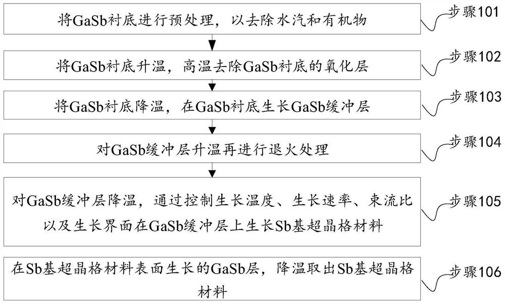
[0029] Such as figure 1 As shown, the method for enhancing the photoluminescence signal of Sb-based superlattice material provided by the present invention comprises the following steps:

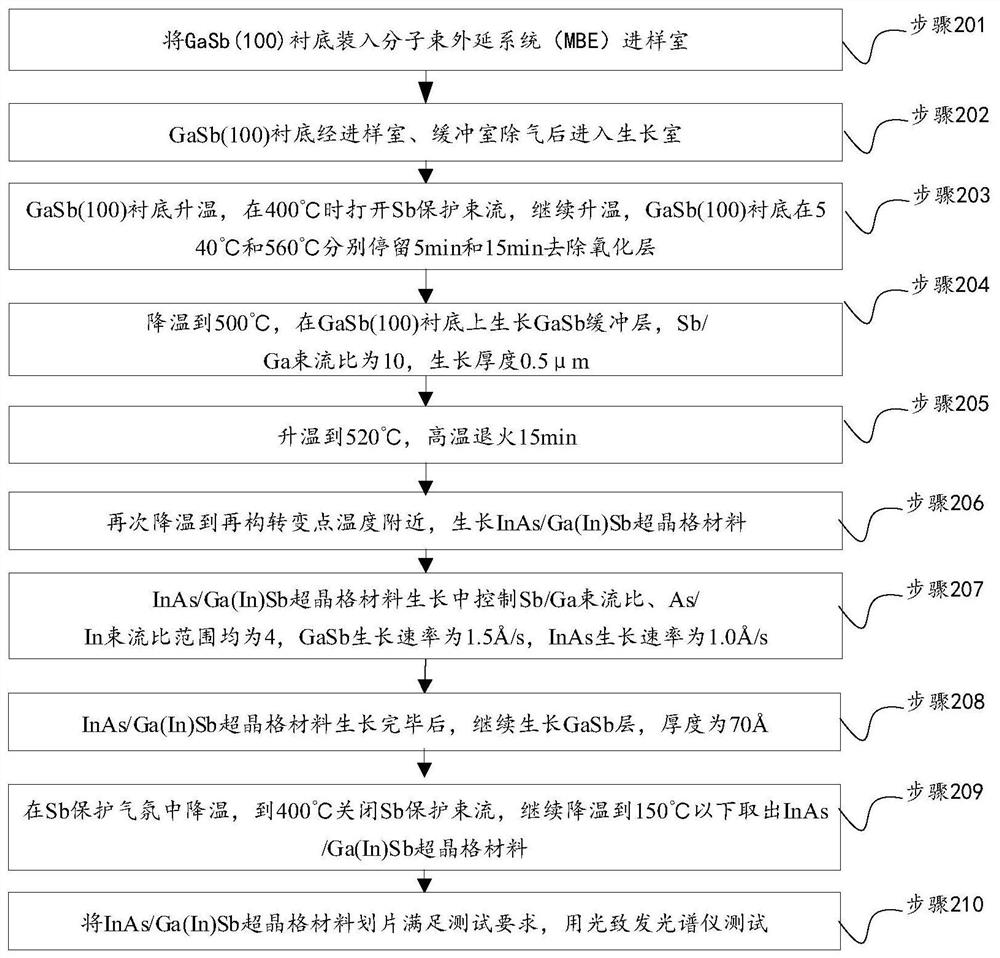
[0030] In step 101, the GaSb substrate is pretreated to remove water vapor and organic matter. In this step, a GaSb (100) substrate is used as the GaSb substrate. The GaSb(100) substrate is loaded into the sample chamber of the molecular beam epitaxy system (MBE), and afte...


PUM

PropertyMeasurementUnit
thicknessaaaaaaaaaa
thicknessaaaaaaaaaa

Abstract

The invention discloses a method for enhancing the photoluminescent signal of an antimony-based superlattice material, comprising: pretreating a GaSb substrate to remove water vapor and organic matter; raising the temperature of the GaSb substrate to remove the oxide layer of the GaSb substrate at high temperature; Cool the GaSb substrate and grow a GaSb buffer layer on the GaSb substrate; heat up the GaSb buffer layer and then anneal; cool down the GaSb buffer layer, and control the growth temperature, growth rate, beam current ratio and growth interface on the GaSb buffer layer Growing the Sb-based superlattice material; growing the GaSb layer on the surface of the Sb-based superlattice material, cooling the Sb-based superlattice material. In the present invention, by performing a photoluminescence test on the Sb-based superlattice material, the photoluminescent signal is greatly enhanced, the peak position of the luminescence is clear, and the half-peak width is small, and the band gap of the superlattice material can be accurately tested, so that the Sb-based superlattice Lattice materials can be widely used in infrared optoelectronic devices to improve the detection accuracy of infrared optoelectronic devices.

Description

technical field [0001] The invention relates to the technical field of semiconductor infrared detectors, in particular to a method for enhancing photoluminescent signals of Sb-based superlattice materials. Background technique [0002] Infrared thermal imaging has the characteristics of strong anti-interference, long recognition distance, and thermal radiation detection. In recent years, it has been widely used in the fields of security, industry, medicine, and automatic driving. [0003] Infrared optoelectronic devices use a wide range of materials, metals, insulators and superconductors can be used to make infrared detectors. Among them, the special physical properties of antimony (symbol "Sb")-based superlattice materials are very suitable for the manufacture of infrared optoelectronic devices. Sb-based superlattice infrared detectors can respond to light radiation from near-infrared to short-wave infrared, medium-wave infrared, long-wave infrared and far-infrared throug...

Claims


Application Information

Patent Timeline
Patent Type & Authority Patents(China)
IPC IPC(8): H01L31/18H01L31/0304H01L31/0352H01L31/102
CPCH01L31/184H01L31/1844H01L31/0304H01L31/03046H01L31/035236H01L31/102Y02P70/50
Inventor 邢伟荣申晨刘铭周朋李乾
Owner 11TH RES INST OF CHINA ELECTRONICS TECH GROUP CORP
Why Eureka
Try Eureka