Flash memory device and manufacturing method thereof

A flash memory device and manufacturing method technology, applied to semiconductor devices, electrical solid devices, electrical components, etc., can solve problems such as reducing coupling ratio, and achieve the effects of increasing coupling ratio, increasing contact area, and improving performance

Active Publication Date: 2021-03-19
SEMICONDUCTOR MANUFACTURING INTERNATIONAL (BEIJING) CORP +1
View PDF7 Cites 0 Cited by
  • Summary
  • Abstract
  • Description
  • Claims
  • Application Information

AI Technical Summary

Problems solved by technology

However, as the size of flash memory devices continues to shrink, the coupling ratio decreases

Method used


Image

  • Flash memory device and manufacturing method thereof
  • Flash memory device and manufacturing method thereof
  • Flash memory device and manufacturing method thereof

Examples


Embodiment Construction

[0021] The following description provides specific application scenarios and requirements of the application, with the purpose of enabling those skilled in the art to manufacture and use the contents of the application. Various local modifications to the disclosed embodiments will be readily apparent to those skilled in the art, and the general principles defined herein may be applied to other embodiments and embodiments without departing from the spirit and scope of the disclosure. application. Thus, the present disclosure is not limited to the embodiments shown, but is to be accorded the widest scope consistent with the claims.

[0022] The technical solution of the present invention will be described in detail below in conjunction with the embodiments and the accompanying drawings.

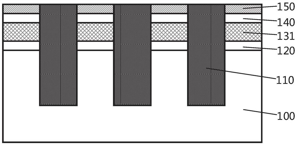
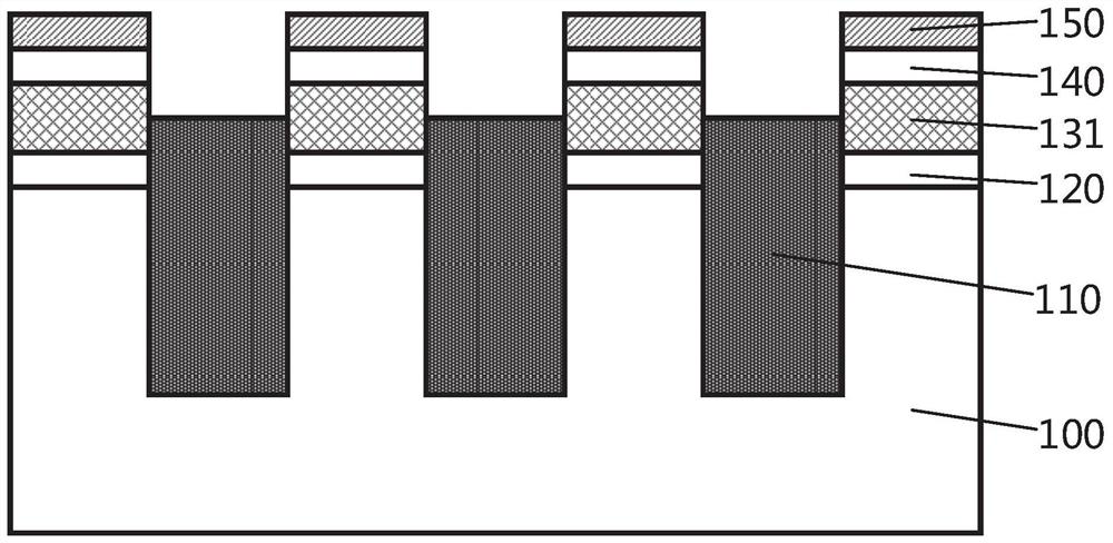
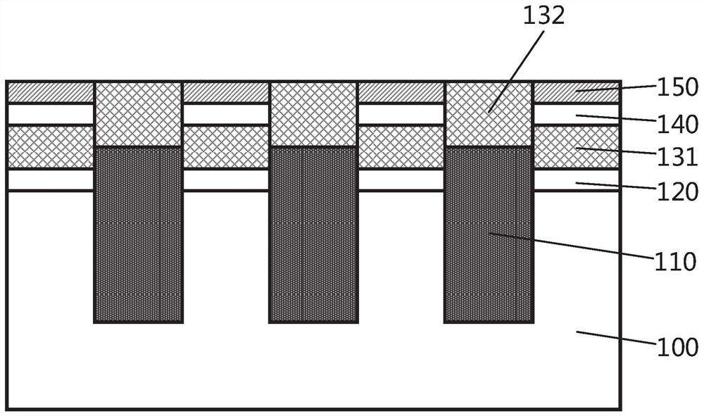
[0023] Figure 1 to Figure 10 It is a schematic structural diagram of each step of the flash memory device manufacturing method described in the embodiment of the present application. Combine...


PUM


Abstract

The invention relates to the field of semiconductor manufacturing, in particular to a flash memory device and a manufacturing method thereof. The flash memory device comprises: a semiconductor substrate; an isolation structure, which is located in the semiconductor substrate and isolates the active region of the semiconductor substrate; a tunneling oxide layer and a floating gate are located on anactive region of the semiconductor substrate, wherein the side wall of the top of the floating gate comprises a protruding structure; a control gate dielectric layer, which is positioned on the surface of the isolation structure and the surface of the floating gate; and a control gate, which is positioned between the floating gates and covers the surface of the control gate dielectric layer. Withthe protruding structure, a contact area between the floating gate and the control gate is increased, a coupling ratio of the device is effectively increased, and the performance of the device is further improved.

Description

technical field [0001] The present application relates to the field of semiconductor manufacturing, in particular to a flash memory device and a manufacturing method thereof. Background technique [0002] In the current semiconductor industry, integrated circuit products can be mainly divided into three types: logic, memory and analog circuits, among which memory devices account for a considerable proportion of integrated circuit products. Among storage devices, flash memory (flash memory for short) has become a mainstream of non-volatile memory. [0003] Flash memory can be divided into two types: floating gate flash memory (floating gate Flash) and charge-trapping memory structure flash memory (CTF, charge-trapping Flash). For the floating gate structure flash memory, due to the existence of the floating gate, the flash memory can complete the reading, writing, and erasing of information. Even in the absence of power supply, the existence of the floating gate can maintain...

Claims


Application Information

Patent Timeline
IPC IPC(8): H01L27/11529H01L27/11536H01L27/11548H01L27/11558
CPCH10B41/41H10B41/44H10B41/50H10B41/60
Inventor 陈建奇
Owner SEMICONDUCTOR MANUFACTURING INTERNATIONAL (BEIJING) CORP
Why Eureka
Try Eureka