Optical thin film deposition device and method
A deposition equipment and optical thin film technology, applied in gaseous chemical plating, metal material coating process, coating and other directions, can solve the problems of deformation of the substrate to be plated, film peeling off, affecting the film deposition effect, etc., to improve the accuracy , the effect of reducing stress
- Summary
- Abstract
- Description
- Claims
- Application Information
AI Technical Summary
Problems solved by technology
Method used
Image

Examples
Embodiment Construction
[0049] The technical solutions in the embodiments of the present invention will be clearly and completely described below in conjunction with the drawings in the present invention. Apparently, the described embodiments are only some of the embodiments of the present invention, not all of them. Based on the embodiments of the present invention, all other embodiments obtained by persons of ordinary skill in the art without making creative efforts belong to the protection scope of the present invention.
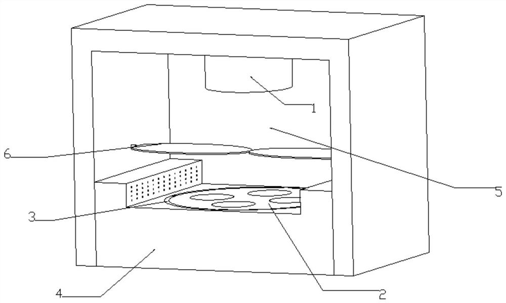
[0050] Such as figure 1 As shown, an optical thin film deposition device disclosed in the present invention includes an ion source 1 , a substrate fixture 2 , a fixture base 3 , a base fixture 4 , a vacuum chamber 5 , and a uniformity correction baffle 6 . The ion source 1 is located on the top of the vacuum chamber 5, the ion source 1 is a radio frequency ion source, the substrate fixture 2 is placed under the ion source 1, the substrate fixture 2 is placed on the upper part of...
PUM
 Abstract
Description
Claims
Application Information