
Uncooled infrared detector and pixel-level packaging structure thereof

A packaging structure, pixel-level technology, applied in electrical radiation detectors and other directions, can solve the problems of inability to achieve the inhalation effect, affecting the overall performance of the detector, and achieve the effect of increasing the inhalation effect, good vacuum, and enhanced performance.

Active Publication Date: 2021-03-23
WUHAN GAOXIN TECH
View PDF12 Cites 0 Cited by
  • Summary
  • Abstract
  • Description
  • Claims
  • Application Information

AI Technical Summary

Problems solved by technology

However, the existing pixel-level packaging technology has a lot of difficulty in sealing the vent hole, because the difficulty of pixel-level packaging lies in how to seal the vent hole in a high vacuum environment and how to ensure the uniformity of the sealing hole and consistency, because only by ensuring the uniformity of the sealing hole can the consistency of the detector responsivity be guaranteed, and if the sealing hole is uneven, it will affect the overall performance of the detector
In addition, the detector uses a getter to absorb air in the vacuum space. However, the existing getters are placed in various positions, but they cannot achieve the best air-intake effect.

Method used


Image

  • Uncooled infrared detector and pixel-level packaging structure thereof

Examples


Embodiment Construction

[0022] The following will clearly and completely describe the technical solutions in the embodiments of the present invention with reference to the accompanying drawings in the embodiments of the present invention. Obviously, the described embodiments are only some, not all, embodiments of the present invention. Based on the embodiments of the present invention, all other embodiments obtained by persons of ordinary skill in the art without making creative efforts belong to the protection scope of the present invention.

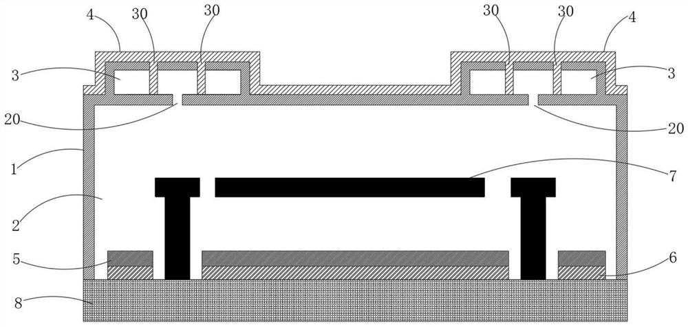
[0023] see figure 1 , the embodiment of the present invention provides a pixel-level packaging structure, including a microcavity 1 arranged on an infrared CMOS readout circuit 8, the microcavity 1 includes a first layer of vacuum space 2 for packaging components and is arranged on the The second layer of vacuum space 3 on the first layer of vacuum space 2; the cavity wall between the first layer of vacuum space 2 and the second layer of vacuum space 3 is prov...


PUM


Abstract

The invention relates to a pixel-level packaging structure comprising a micro-cavity arranged on an infrared CMOS reading circuit; the micro-cavity comprises a first-layer vacuum space for placing a packaging part and a second-layer vacuum space arranged on the first-layer vacuum space; and a first exhaust hole is formed in the cavity wall between the first-layer vacuum space and the second-layervacuum space, two second exhaust holes are formed in the side, away from the first-layer vacuum space, of the second-layer vacuum space, and the first exhaust hole communicates with the two second exhaust holes. The invention further provides an uncooled infrared detector; the uncooled infrared detector further comprises the pixel-level packaging structure, and the micro-cavity is arranged on an infrared CMOS reading circuit. The first exhaust hole and the two second exhaust holes are formed, the three exhaust holes are combined to form a Y-shaped structure, the hole sealing difficulty can begreatly reduced, and thus the hole filling uniformity within the whole 8-inch range is improved, and the overall performance uniformity of the detector is greatly improved.

Description

technical field [0001] The invention relates to the technical field of pixel-level packaging, in particular to an uncooled infrared detector and a pixel-level packaging structure thereof. Background technique [0002] At present, uncooled infrared mostly adopts packaging technology, which can be divided into chip level, wafer level and pixel level, etc. Among them, chip level packaging technology can be divided into metal tube package and ceramic tube package according to the difference of package shell. [0003] Metal shell packaging is the earliest packaging technology adopted, and the technology is very mature. Due to the use of high-cost components such as metal case, TEC and getter, the cost of metal case packaging has been high, which limits its application to low-cost devices. [0004] The ceramic shell package can significantly reduce the volume and weight of the packaged detector, and it is much lower than the traditional metal shell package in terms of raw materia...

Claims


Application Information

Patent Timeline
Patent Type & Authority Applications(China)
IPC IPC(8): G01J5/10
CPCG01J5/10
Inventor 黄立叶帆马占锋曾国胜汪超王春水
Owner WUHAN GAOXIN TECH
Learn More