
Gallium nitride-based high-electron-mobility transistor simulation method and device and storage medium

A high electron mobility, gallium nitride-based technology, applied in the field of semiconductor device simulation, can solve the problems of missing gate reverse current, affecting the model DC and accurate description of large signals, etc.

Pending Publication Date: 2021-03-26
XIAMEN SANAN INTEGRATED CIRCUIT
View PDF6 Cites 0 Cited by
  • Summary
  • Abstract
  • Description
  • Claims
  • Application Information

AI Technical Summary

Problems solved by technology

However, the existing ASM model focuses on describing the trap model and field plate model of GaN devices, but the description of gate reverse current is missing. However, since GaN devices are under negative gate voltage It is turned on, and in existing applications, GaN devices also work under negative gate voltage, so the lack of description of the reverse current will affect the accurate description of the model for DC and large signals

Method used


Image

  • Gallium nitride-based high-electron-mobility transistor simulation method and device and storage medium
  • Gallium nitride-based high-electron-mobility transistor simulation method and device and storage medium
  • Gallium nitride-based high-electron-mobility transistor simulation method and device and storage medium

Examples


no. 1 example

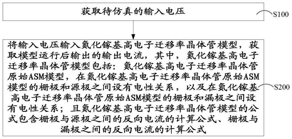
[0035] Please refer to figure 1 , this embodiment provides a simulation method for a gallium nitride-based high electron mobility transistor, and the simulation method for a gallium nitride-based high electron mobility transistor includes the following steps:

[0036] S100. Acquire an input voltage to be simulated.

[0037] It should be noted that the simulation method for GaN-based high electron mobility transistors provided in this embodiment is applied to an intensive model of advanced high electron mobility field effect transistors.

[0038] In addition, those skilled in the art can select the input voltage to be simulated based on the parameters of the gallium nitride-based high electron mobility transistor to be designed. For example, in this embodiment, the above input voltage is the port voltage of the transistor. Wherein, the port voltages respectively include the port voltages of the gate, the source, and the drain.

[0039] S200. Input the input voltage into the G...

no. 2 example

[0092] Compared with the first embodiment, this embodiment differs in that different formulas are used to calculate the reverse current between the gate and the source and the reverse current between the gate and the drain.

[0093] As an example, in this embodiment, the following calculation formula can be used to calculate the reverse current between the gate and the source:

[0094]

[0095] Among them, I gsr is the reverse current between gate and source, C is the first model coefficient, μ is the carrier diffusion mobility, V gs is the voltage across the gate and source, β is the second model coefficient, and PFC is the correction factor. It should be noted that, in this embodiment, the involved parameters C, μ, β, and PFC are all parameters in an existing model (ie, the original ASM model).

[0096] Correspondingly, the correction factor PFC in the above formula can be calculated by the following formula:

[0097]

[0098] Among them, ψ d is the height of the p...


PUM


Abstract

The invention discloses a gallium nitride-based high-electron-mobility transistor simulation method and device and a storage medium, and relates to the technical field of semiconductor device simulation. The method comprises the following steps: acquiring an input voltage to be simulated; inputting input voltage into a GaN-based high-electron-mobility transistor model, acquiring output current output after model operation, wherein the model comprises an original ASM model, an electric relationship is set between a grid electrode and a source electrode of the original ASM model, and an electricrelation is set between the grid electrode and a drain electrode of the original ASM model; and the formula of the model comprises a calculation formula of reverse current between the grid electrodeand the source electrode and a calculation formula of reverse current between the grid electrode and the drain electrode. The gallium nitride-based high-electron-mobility transistor simulation methodcan solve the problem of deficiency of an advanced high-electron-mobility field effect transistor intensive model in description of device gate reverse current, thereby improving the simulation accuracy of the transistor.

Description

technical field [0001] The present invention relates to the technical field of simulation of semiconductor devices, in particular to a simulation method, device and storage medium for gallium nitride-based high electron mobility transistors. Background technique [0002] AlGaN / GaN high electron mobility transistor (High Electron Mobility Transistor, HEMT) has increasingly become the focus of today's RF microwave circuit design due to its characteristics of high power, high current density, high electron saturation velocity and high breakdown electric field. As the miniaturization of integrated circuits continues to increase and the degree of integration continues to increase, people's enthusiasm for monolithic microwave integrated circuit (Monolithic microwave integrated circuit, MMIC) design is gradually increasing. An accurate device model can simulate real device characteristics, help designers understand device characteristics, and also help design tape-out, which is of ...

Claims


Application Information

Patent Timeline
IPC IPC(8): G06F30/367
CPCG06F30/367Y02B70/10
Inventor 张永明蔡文必魏鸿基林义书
Owner XIAMEN SANAN INTEGRATED CIRCUIT
Learn More