[0027] The present invention is described below based on the examples, but the present invention is not limited to these examples. In the detailed description of the invention, some particular detail portions are described in detail. The description of these detail portions can also be fully understood in the art. In order to avoid obscuring the substance of the present invention, the methods, processes, processes, components, and circuits are not described in detail.
[0028] In addition, one of ordinary skill in the art will appreciate that the accompanying drawings herein are for illustrative purposes, and the accompanying drawings are not necessarily drawn.
[0029] At the same time, it should be understood that in the following description, "circuit" refers to a conductive circuit composed of at least one element or sub-circuit through an electrical connection or electromagnetic connection. When an element or circuit "connected to" other element or "connected" connection element / circuit "connected between" two nodes, it may be directly coupled or connected to another element or may exist between intermediate components, components. The connection can be physical, logically, or thereon. In contrast, when the component "directly coupled to" or "directly connected to" other elements, it means that there is no intermediate element.
[0030] Unless the context clear requests, "including", "including", "including", "including", "including", "including", "including", "including", "including", "including", "includes", "includes" including, but not limited to ", unless the meaning of the specification and claims should be interpreted rather than exciting Meaning.
[0031] In the description of the invention, it is to be understood that the terms "first", "second", etc. are used only to describe purposes, and cannot be understood as instructions or implies relative importance. Moreover, in the description of the invention, the meaning of "multiple" is two or more unless otherwise stated.
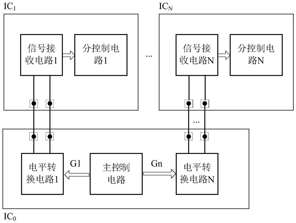
[0032] figure 1 A structural diagram of the first communication control circuit according to an embodiment of the present invention. Such as figure 1 As shown, the communication control circuit includes a master wafer IC 0 And multiple controlled wafers. Main control wafer IC 0 Includes main control circuits and multiple level conversion circuits. In this embodiment, the main control wafer IC 0 The N level conversion circuit includes an example, where n is a positive integer. In the present embodiment, the number of level conversion circuits corresponds to the number of the partition wafer. In the present embodiment, the communication control circuit includes n-control wafer ICs. 1 -IC N Each stereotyped wafer is used to receive the main control wafer IC 0 The transmitted control information is different from the corresponding control, and the reference to the n-controlled wafer is different. Further, each of the partition wafers includes a point control circuit. It should be noted that the reference ground of the controlled wafer is also different from each other.
[0033] Furthermore, it should be understood that the main control circuit and the sub-control circuit mentioned in the present invention may be a circuit that implements any control function, which can generate different control signals to control other circuit parts, such as drive control circuitry, feedback control circuitry, such as driving control circuitry , Protection circuit, etc., this is not limited.
[0034] Further, each of the controlled wafers also includes a signal receiving circuit for receiving the main control wafer IC. 0 The corresponding level conversion circuit passes the signal, and converts the signal required to control the circuit. In this embodiment, the controlled wafer IC 1 Includes signal receiving circuit 1 and split control circuit 1, ..., controlled wafer IC N A signal receiving circuit N and a split control circuit N are included.
[0035] Specifically, the main control wafer IC 0 And controlled wafer IC 1 Communication between communication is an example, and other controllants communicate with the main control wafer are the same. The level conversion circuit 1 is used to convert the level of the control signal G1 transmitted by the main control circuit to the controlled wafer IC. 1 Received level to achieve the main control wafer IC 0 And controlled wafer IC 1 Communication between. It should be understood that the level of the control signal G1 generated by the main control circuit is relative to the main control wafer IC. 0 In the reference place, when it passes the different partial control wafer IC 1 When the level of the signal needs to be converted to control the controlled wafer IC after conversion 1 The circuit in the middle.
[0036] At the same time, the maximum pressure resistant to the device in the level conversion circuit 1 is the main control wafer IC. 0 And controlled wafer IC 1 The maximum pressure difference between the two levels, so that the high pressure is only affected by the level conversion circuit, and due to the controlled wafer IC 1 With the main wafer IC 0 Leave, with high voltage level conversion circuit integrate in the main control wafer IC 0 There is no need to use the high pressure isolation ring, that is, although the main control wafer IC 0 Including the level conversion circuit with high pressure, but it does not require a high pressure isolation ring, there is no need to have an epitaxial layer, thus reducing the production cost and process difficulty of the wafer, and greatly reduces the area of the wafer. Of course, any of the prior art can achieve the above-described level conversion circuitry can be applied in the present invention, which is not limited thereto.
[0037] Such as figure 1 Description, the main control wafer IC 0 The plurality of level conversion circuits 1-n are each pass or reassigned, respectively, and the controlled wafer IC, respectively. 1 -IC N The signal receiving circuit in the middle corresponds to the connection, it should be understood that the connection between the wafers is not limited thereto. In this embodiment, the main control wafer IC 0 And controlled wafer IC 1 -IC N Finally packaged in the same chip. Here, there is no need for the presence of a high pressure isolation ring between the different control circuits, and thus the volume of the chip after the package is greatly reduced.
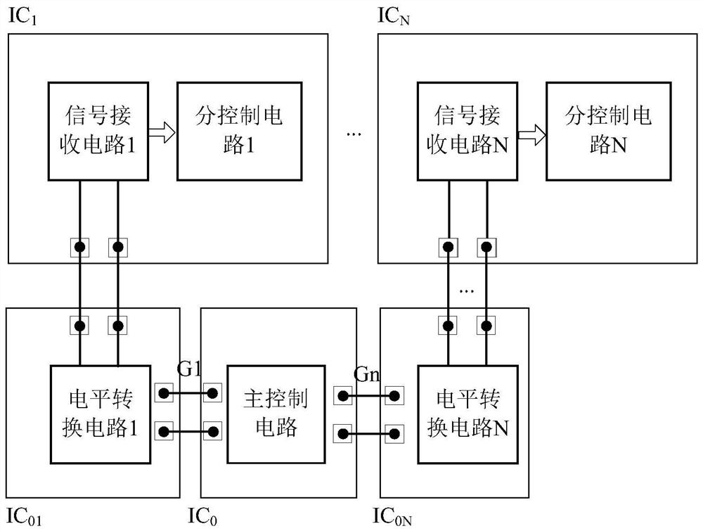
[0038]figure 2 A structural diagram of the second communication control circuit of the embodiment of the present invention is given. Such as figure 2 As shown, the communication control circuit includes a master wafer IC 0 , Multiple control wafers and plurality of conversion wafers, wherein the number of converted wafers corresponds to equal to the number of control wafers. In the present embodiment, both the control wafer and the conversion wafer are N as an example, n is a positive integer. Main control wafer IC 0 Includes main control circuitry for generating various control signals. Erogate wafer IC 1 -IC N The structure is the same as that of the above embodiments, and will not be explained herein. the difference is, figure 1 Main control wafer IC 0 Each level conversion circuit is separately used as a wafer, ie the conversion wafer IC 01 -IC 0N. Due to level conversion circuit and main control wafer IC 0 Separate, thus level conversion circuit 1-N passes the wire or the reassocial layer and the main control wafer IC 0 The main control circuit is connected to the control signal G1-GN transmitted to the main control circuit transmission. Similarly, conversion wafer IC 01 -IC 0N The level conversion circuit 1-n is respectively passed through the wire or the reassignment layer and the control wafer IC, respectively. 1 -IC N The signal receiving circuit 1-N corresponds to the main control wafer IC. 0 The level of transmitted control signals G1-GN is converted to the controlled wafer IC 1 -IC N The level of receiving, thereby realizing the main control wafer IC 0 And various control wafers IC 1 -IC N Communication between.
[0039] In the present embodiment, the level conversion circuit is separately used as a conversion wafer such that the level conversion circuit similar to the function can only design a conversion wafer, and a complex function can be achieved by placing a plurality of the same conversion wafers. It is conducive to modular design.
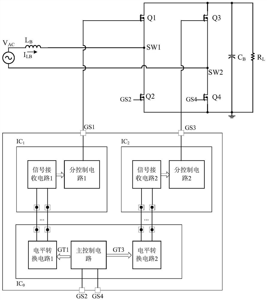
[0040] image 3 A schematic diagram of a communication control circuit applied to the first power supply circuit is given in accordance with an embodiment of the present invention. As shown, here is only figure 1 The communication control circuit shown is illustrated as an example. It should be understood that the second communication control circuit is also applicable.
[0041] In the present embodiment, the bridgeable PFC circuit includes parallel connection R L Two bridge arms between the two ends, wherein the first bridge arm includes a series connected power tube Q1 and power tube Q2, and the second bridge arm includes power tubes Q3 and Q4 connected in series, and at the same time, AC input voltage V AC The first end is inductively L B The common node SW1 connected to the power tubes Q1 and Q2 is connected to the second end of the AC input voltage VA to connect to the common node SW2 of the power tubes Q3 and Q4. Here, the power tube Q1 and Q2 are controlled by the high frequency PWM pulse signal to perform switching operations, power tubes Q3 and Q4 are controlled by the switching operation to perform switching operations. It will be understood that other control methods in the prior art can also be applied thereby, and the present invention will not be limited.
[0042] Since the drive floating of power tubes Q1 and Q3, if a conventional drive control circuit is employed, the control wafer needs to be isolated using a high pressure isolation ring, occupying a large amount of wafer area. The protocol circuit and two level conversion circuits are designed on a wafer (ie, the main control wafer IC) using the scheme of the embodiment of the present invention. 0 Further, the split control circuit 1 (here, driving control circuit 1) and the signal receiving circuit 1 are designed on a wafer (ie, the stencil IC). 1 ), The split control circuit 2 (here, driving control circuit 2) and the signal receiving circuit 2 are designed on a wafer (ie, the controlled wafer IC) (ie, the controlled wafer IC) corresponding to the power tube Q2. 2 ), Isolation can be achieved without the use of high pressure isolation loops.
[0043] In the present embodiment, the main control circuit is used to generate a logical drive signal of each power tube (Q1-Q4), the level conversion circuit 1 receives the logical drive signal GT1, and converts it to the controlled wafer IC. 1 Level signal. The signal receiving circuit 1 receives the signal and converts it to control the signal of the drive control circuit 1 such that the drive control circuit 1 outputs the drive signal GS1 of the power tube Q1. Similarly, the level conversion circuit 2 receives the logical drive signal GT3, and converts it to the controlled wafer IC. 2 Level signal. The signal receiving circuit 2 receives the signal and converts it into a signal capable of controlling the drive control circuit 2 such that the drive signal GS3 of the power tube Q3 is output. Since the power tubes Q2 and Q4 are grounded, the corresponding driving control circuits are disposed in the main control circuit to directly generate drive signals GS2 and GS4 of power tubes Q2 and Q4.
[0044] In some embodiments, each level conversion circuit can include two switching tubes, each switching pipe controlled on or off, and the first power end of each switch tube is controlled according to the control signal output by the main control circuit. The high voltage power supply of the control wafer is connected, and the second power end is connected to the reference ground of the main control circuit, thereby only by the switch tube to withstand the high pressure pressure difference. Therefore, the part control wafer itself can be produced by low pressure process, and due to the separation of the control wafer and the main control wafer, the high-pressure switching tube is integrated in the main control wafer, which is not required to use the high voltage isolation ring, that is, although the main control wafer includes tolerance High-pressure switching tubes, but it does not require a high pressure isolation ring, and does not require the process of epitaxial layer, thereby reducing the production cost and process difficulty of wafer, and greatly reduces the area of the wafer.
[0045] In the present embodiment, the function and implementation of the level conversion circuits 1 and 2 are the same, so that only the wafer of a level conversion circuit can be designed, such as figure 2 The architecture of the second communication control circuit shown separately separates the level conversion circuit, simplifies the circuit design by placing a plurality of the same wafers.
[0046] Figure 4 A schematic diagram of a communication control circuit applied to the second power supply circuit is given. Figure 4 A bridgeless PFC with interleaved parallel is given to further reduce current ripple. As shown, the bridge PFC includes parallel connection R L A plurality of bridge arms at both ends, which will be described using three bridge arms as an example. AC input voltage V AC The first end is inductively L B1 Connect to the common node SW1 SW1 of the power tube Q1 and Q2 in the first bridge arm, and the first end is also inductively L. B2 Connect to the common node SW2 SW2 of power tube Q3 and Q4 in the second bridge arm; AC input voltage V AC The second end is connected to the common node SW3 of the power tube Q5 and Q6 in the third bridge arm. In the present embodiment, since the upper power tubes (Q1, Q3 and Q5) of the plurality of bridge arms are all different, the reference to the respective upper power tubes correspond to the reference grounds.
[0047] In this embodiment, the main control wafer IC 0 The main control circuit is used to generate a logical drive signal of each power tube. The sub-control circuit and signal receiving circuit corresponding to the upper power tube of each bridge arm are designed on a wafer to form a plurality of controlled wafers IC. 1 -IC 3 Each of the control wafers is separated from the main control wafer, thereby avoiding the use of the high pressure isolation ring, which greatly saves the wafer area and reduces the wafer cost. At the same time, since each of the controlled wafers is used in the present embodiment to drive the upper power tube of each bridge, the structures and the implementation of the implementation are the same, therefore, therefore, it is possible to communicate between control circuits for different reference grounds. The level conversion circuit is separately designed on a wafer, i.e., only a conversion wafer including a level conversion circuit, thereby being controlled by placing a plurality of conversion wafers to achieve a plurality of upper power tubes.
[0048] Such as Figure 4 As shown, the level conversion circuit 1-3 is placed in the conversion wafer IC, respectively. 01 -IC 03 In order to receive the logical drive signals GT1, GT3, and GT5 from the main control circuit, and convert it to the corresponding control wafer IC, respectively. 1 -IC 3 Level signal. Specifically, the level conversion circuit 1 receives the logical drive signal GT1 and converts it to the controlled wafer IC. 1 Level signal. The signal receiving circuit 1 receives the signal and converts it to control the signal of the drive control circuit 1 such that the drive control circuit 1 outputs the drive signal GS1 of the power tube Q1. The generation of the drive signal GS3 and GS5 is hereby incorporated herein by reference.
[0049] Since the lower power tube (Q2, Q4 and Q6) of each bridge arm is connected to the ground level, the corresponding driving control circuit is disposed in the main control circuit to directly generate drive signals of power tubes Q2, Q4 and Q6. GS2, GS4 and GS6.
[0050] The power supply circuit of the embodiment of the present invention will be described only by no bridge PFC circuit, and it is understood that the power supply circuits of the power tube including different reference ground can be applied. Further, the circuit of the communication control circuit of the embodiment of the present invention can be applied to the circuitry of the control signals of different references.
[0051] It is not intended to limit the invention and is not intended to limit the invention, and those skilled in the art may have various changes and variations. Any modification, equivalent replacement, improvement, etc. according to the spirit and principles of the present invention should be included within the scope of the invention.