Ultrasonic fingerprint sensing chip, electronic equipment and manufacturing method

A technology for sensing chips and manufacturing methods, which are applied in the fields of acquiring/arranging fingerprints/palmprints, manufacturing microstructure devices, decorative arts, etc. The effect of density and fingerprint recognition performance

Pending Publication Date: 2021-03-30
SILEAD
View PDF0 Cites 1 Cited by
  • Summary
  • Abstract
  • Description
  • Claims
  • Application Information

AI Technical Summary

Problems solved by technology

However, the optical fingerprint recognition technology mainly collects the skin texture of the finger, which has poor anti-counterfeiting performance. Moreover, both the optical fingerprint recognition technology and the capacitive fingerprint recognition technology have poor recognition effects on wet fingers.

Method used


Image

  • Ultrasonic fingerprint sensing chip, electronic equipment and manufacturing method
  • Ultrasonic fingerprint sensing chip, electronic equipment and manufacturing method
  • Ultrasonic fingerprint sensing chip, electronic equipment and manufacturing method

Examples


Embodiment 1

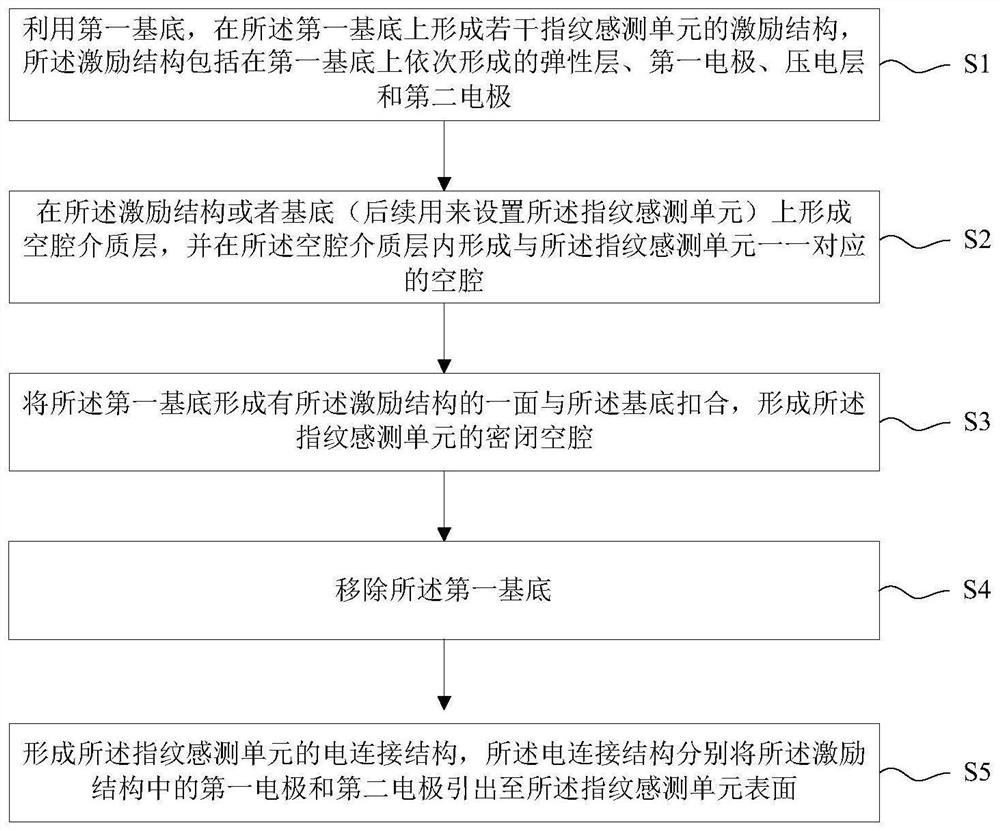
[0053] Figure 2A to Figure 2N It is a schematic cross-sectional structure diagram during the manufacturing process of the manufacturing method of the ultrasonic fingerprint sensing chip according to Embodiment 1 of the present invention. Refer to the following figure 1 with Figure 2A to Figure 2N , the manufacturing method of the ultrasonic fingerprint sensing chip according to Embodiment 1 of the present invention will be described.

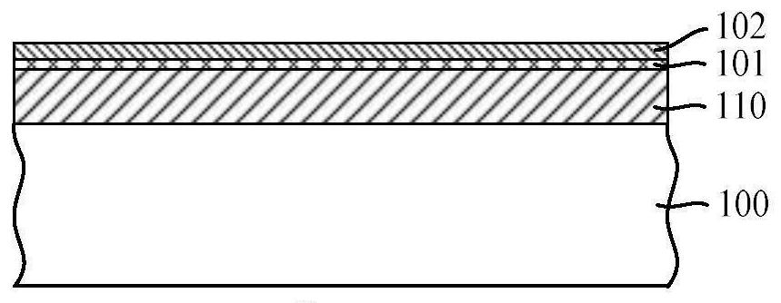
[0054] see Figure 2D The manufacturing method of the ultrasonic fingerprint sensing chip of this embodiment includes step S1, providing a first substrate 100, and forming a plurality of excitation structures 10 of fingerprint sensing units on the first substrate 100, and the excitation structure 10 is included in the first substrate 100. The elastic layer 110 , the first electrode 120 , the piezoelectric layer 130 and the second electrode 140 are sequentially formed on the first substrate 100 .

[0055] The material of the first substrate...

Embodiment 2

[0091] This embodiment relates to a manufacturing method of an ultrasonic fingerprint sensing chip. The main difference between this embodiment and the first embodiment lies in the method of forming the cavity.

[0092] This example is in Figure 2D The manufacturing method of the ultrasonic fingerprint sensing chip is further described on the basis of the process after the second electrode is formed. This embodiment may include the following: Figure 2A to Figure 2D The production process shown. Figure 3A to Figure 3D It is a schematic cross-sectional structure diagram during the manufacturing process of the manufacturing method of the ultrasonic fingerprint sensing chip according to the second embodiment of the present invention. The following main combination Figure 3A to Figure 3D The fabrication method of the ultrasonic fingerprint sensing chip of this embodiment will be described.

[0093] see Figure 3A Firstly, corresponding to the cavity area CA where the cavit...

Embodiment 3

[0099] This embodiment relates to a manufacturing method of an ultrasonic fingerprint sensing chip. The main difference between this embodiment and Embodiment 1 and Embodiment 2 lies in the method of forming the cavity.

[0100] This example is in Figure 2D The manufacturing method of the ultrasonic fingerprint sensor chip is further described on the basis of the process after the second electrode is formed, and this embodiment may also include the following: Figure 2A to Figure 2D The production process shown. Figure 4A to Figure 4E It is a schematic cross-sectional structure diagram during the manufacturing process of the manufacturing method of the ultrasonic fingerprint sensing chip according to the third embodiment of the present invention. The following main combination Figure 4A to Figure 4E The fabrication method of the ultrasonic fingerprint sensing chip of this embodiment will be described.

[0101] First, see Figure 4A , a cavity defining layer 107 is form...


PUM

PropertyMeasurementUnit
thicknessaaaaaaaaaa
thicknessaaaaaaaaaa
thicknessaaaaaaaaaa

Abstract

The invention relates to an ultrasonic fingerprint sensing chip, electronic equipment with a fingerprint recognition function and a manufacturing method. According to the manufacturing method, an excitation structure of the fingerprint sensing unit is formed on a first substrate, a corresponding cavity is formed on the excitation structure or another substrate, then the two substrates are buckledto form a closed cavity of the fingerprint sensing unit, and after the first substrate is removed, an electric connection structure is formed to lead a first electrode and a second electrode in the excitation structure to the surface. The formed ultrasonic fingerprint sensing chip comprises a plurality of fingerprint sensing units obtained through the method for fingerprint recognition, each fingerprint sensing unit is compact in structure, and the design density and the fingerprint recognition performance of the fingerprint sensing units can be improved.

Description

technical field [0001] The invention relates to the technical field of semiconductor manufacturing, in particular to an ultrasonic fingerprint sensing chip and a manufacturing method thereof, and an electronic device with a fingerprint identification function. Background technique [0002] At present, fingerprint recognition technology has become one of the hot spots in the field of biometrics, and is widely used in various applications involving user information verification such as consumer electronics, access control systems, and information collection. Taking the fingerprint recognition technology applied to mobile terminals as an example, the capacitive fingerprint recognition technology currently occupies the mainstream. However, with the industry's demand for full-screen mobile phones, fingerprint recognition requires that it can penetrate a medium layer (such as glass) with a thickness of more than 1mm. , metal, plastic, or display and glass). This requirement is a ...

Claims


Application Information

Patent Timeline
Patent Type & Authority Applications(China)
IPC IPC(8): G06K9/00B81C1/00
CPCB81C1/00047G06V40/1306
Inventor 黄景泽梁骥效烨辉程泰毅
Owner SILEAD
Why Eureka
Try Eureka