Manufacturing method of electroplated metal wire

A manufacturing method and a technology of electroplating metal, which are applied in the manufacture of printed circuits, printed circuits, electrical components, etc., can solve the problems of high technical strength and difficulty in manufacturing

Pending Publication Date: 2021-03-30
恒煦电子材料国际有限公司
View PDF10 Cites 0 Cited by
  • Summary
  • Abstract
  • Description
  • Claims
  • Application Information

AI Technical Summary

Problems solved by technology

This kind of process uses the technology of double-layer photoresist. To expose and develop the double-layer photoresist at the same time requires high technical strength and is not easy to manufacture.

Method used


Image

  • Manufacturing method of electroplated metal wire
  • Manufacturing method of electroplated metal wire
  • Manufacturing method of electroplated metal wire

Examples


Embodiment Construction

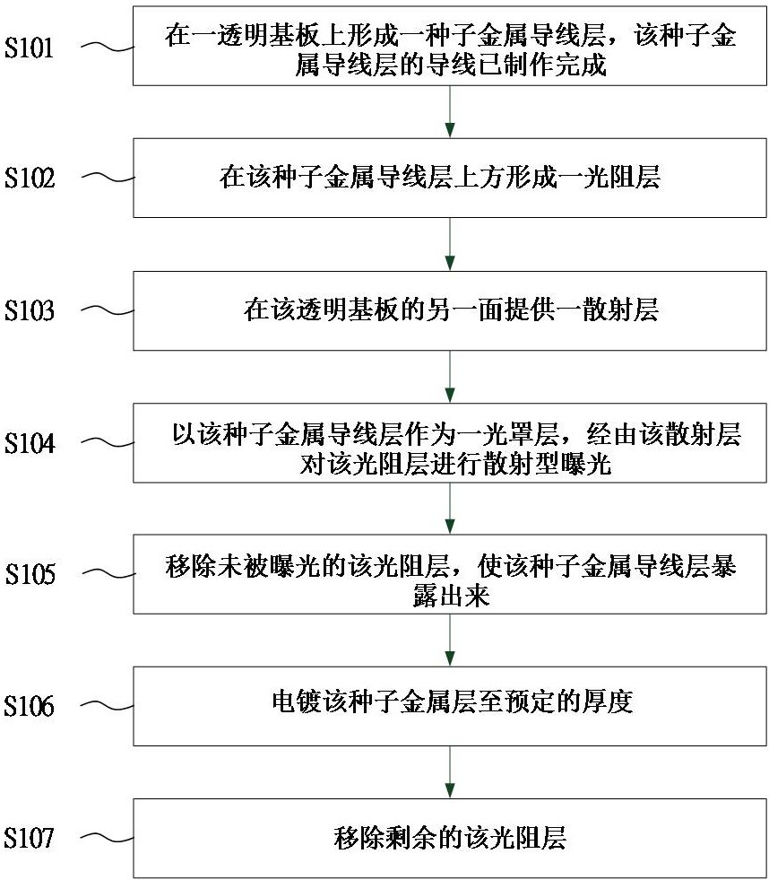
[0031] According to an embodiment of the present invention, the present invention uses the prepared metal wire seed layer as a photomask, and simultaneously uses a scattering layer as an auxiliary layer for back exposure, so as to solve the problem of exposure when the metal wire seed layer is used as a photomask. Diffraction problems will occur, and the structure required for exposure to the negative photoresist can be accurately fabricated. The manufacturing process is simple, easy to implement, and low in cost, which greatly improves the yield of the high aspect ratio electroplating process.

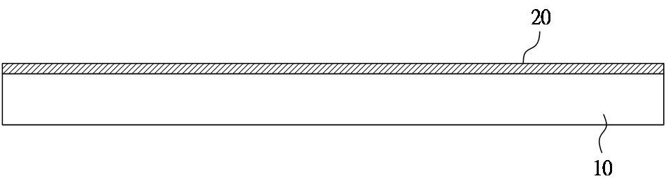
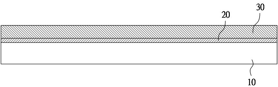
[0032] Please refer to figure 1 , a method for making an electroplated metal wire disclosed in the present invention, please refer to Figures 2A-2L , Figures 3A-3K An embodiment of the production process, including:

[0033] Step S101 : forming a seed metal wire layer on a transparent substrate, and the wires of the seed metal wire layer have been fabricated. There are two method...


PUM

PropertyMeasurementUnit
widthaaaaaaaaaa
thicknessaaaaaaaaaa
thicknessaaaaaaaaaa

Abstract

The invention discloses a method for manufacturing an electroplated metal wire, and the method comprises the following steps: forming a sub-metal wire layer on a transparent substrate, and finishing the manufacturing of the wire of the sub-metal wire layer; forming a photoresist layer above the seed metal wire layer; providing a scattering layer on the other surface of the transparent substrate; taking the seed metal wire layer as a photomask layer, and performing scattering type exposure on the photoresist layer through the scattering layer; removing the unexposed photoresist layer to exposethe seed metal wire layer; electroplating the seed metal wire layer to a predetermined thickness to form a metal wire layer; and removing the remaining photoresist layer. The method is simple in process, easy to implement and low in cost, and the yield of the high aspect ratio electroplating process is greatly improved.

Description

technical field [0001] The invention relates to an electroplating metal technology, in particular to a method for making an electroplating metal wire. Background technique [0002] With the rapid development of portable electronic devices, the miniaturization of components, the reduction of circuit board line width, the improvement of precision, and the reduction of power consumption have made high-aspect-ratio copper electroplating process become a popular science. [0003] At present, the copper electroplating process with high aspect ratio can achieve a line width of 1 micron to 15 micron and a thickness of 10 micron to 100 micron. However, in order to achieve such precision, it must be realized through exposure and development process. In order to make high-aspect-ratio copper wires, it is necessary to form an extremely thin seed copper metal layer on the substrate, and then go through processes such as forming a photoresist layer, exposing and developing, electroplatin...

Claims


Application Information

Patent Timeline
Patent Type & Authority Applications(China)
IPC IPC(8): H05K3/20
CPCH05K3/205H05K2203/056
Inventor 许铭案谢东宏陈香婷
Owner 恒煦电子材料国际有限公司
Why Eureka
Try Eureka