Color film substrate, manufacturing method of color film substrate and display panel

A color film substrate and display area technology, applied in nonlinear optics, instruments, optics, etc., can solve the problem of uneven thickness of the box around the display panel

Inactive Publication Date: 2021-04-02
HKC CORP LTD
View PDF6 Cites 1 Cited by
  • Summary
  • Abstract
  • Description
  • Claims
  • Application Information

AI Technical Summary

Problems solved by technology

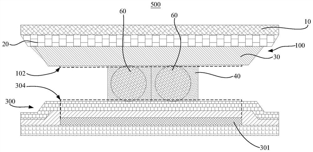
The selection of the space ball is a fixed particle size. When the space ball particle size is calculated on the vertical plane where the non-display A area (double-layer metal line area) is located, for the non-display B area (single-layer metal line area), The particle size of the space ball is relatively small; when the particle size of the space ball is calculated on the vertical surface where the non-display area B is located, the particle size of the space ball is relatively large for the non-display area A, which will easily lead to uneven thickness of the box around the display panel

Method used


Image

  • Color film substrate, manufacturing method of color film substrate and display panel
  • Color film substrate, manufacturing method of color film substrate and display panel
  • Color film substrate, manufacturing method of color film substrate and display panel

Examples


Embodiment Construction

[0041] The following will clearly and completely describe the technical solutions in the embodiments of the present invention with reference to the accompanying drawings in the embodiments of the present invention. Obviously, the described embodiments are only part of the embodiments of the present invention, not all of them. Based on the embodiments of the present invention, all other embodiments obtained by persons of ordinary skill in the art without creative efforts fall within the protection scope of the present invention.

[0042] It should be noted that all directional indications (such as up, down, left, right, front, back...) in the embodiments of the present invention are only used to explain the relationship between the components in a certain posture (as shown in the accompanying drawings). Relative positional relationship, movement conditions, etc., if the specific posture changes, the directional indication will also change accordingly.

[0043] In addition, the ...


PUM


Abstract

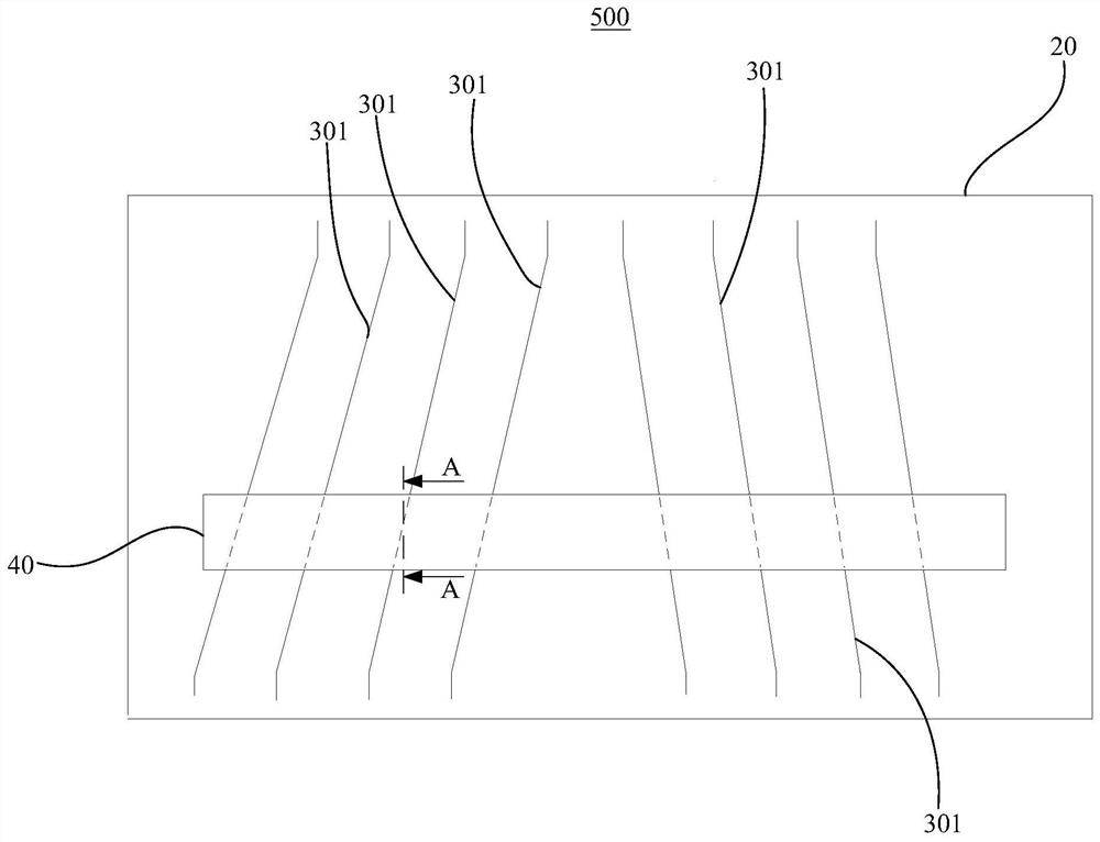
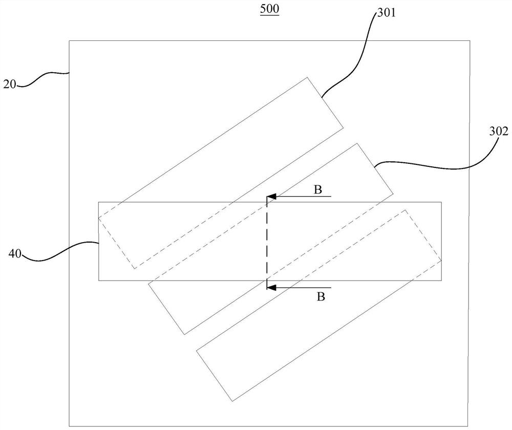
The invention discloses a color film substrate, a manufacturing method of the color film substrate and a display panel, the color film substrate is provided with a display area and a non-display areasurrounding the display area, and the non-display area is defined to comprise a first non-display area right opposite to a double-layer metal wiring area of an array substrate and a second non-displayarea right opposite to a single-layer metal wiring area of the array substrate. The color film substrate further comprises: a substrate body; a black matrix layer which is arranged on one surface ofthe substrate body, wherein a first receding groove is formed in the surface, deviating from the substrate body, of the black matrix layer, and the first receding groove is located in the first non-display area; and a conducting layer which is arranged on the side, deviating from the substrate, of the black matrix layer, wherein at least part of the conducting layer is sunken in the first recedinggroove to form a second receding groove. According to the technical scheme, when the particle size of the gap supporting ball is calculated according to the longitudinal sections of the first non-display area and the second non-display area, the particle size of the gap supporting ball is uniform, and then it is guaranteed that the box thickness of the display panel is uniform.

Description

technical field [0001] The present invention relates to the technical field of display panels, in particular to a color filter substrate, a manufacturing method of the color filter substrate, and a display panel. Background technique [0002] A liquid crystal display panel (Liquid Crystal Display, LCD) is widely used due to many advantages such as a thin body, power saving, and no radiation. The TFT-LCD manufacturing process includes array manufacturing engineering, color film manufacturing engineering and liquid crystal cell manufacturing engineering. Among them, the liquid crystal cell manufacturing engineering is transferred to the liquid crystal cell engineering after the array and color film manufacturing processes are completed. The main process of liquid crystal cell manufacturing includes coating of liquid crystal alignment layer, liquid crystal dripping, coating of edge sealing frame glue, coating of gold balls, vacuum assembly into cells, cutting, etc. The coating...

Claims


Application Information

Patent Timeline
Patent Type & Authority Applications(China)
IPC IPC(8): G02F1/1335G02F1/1339
CPCG02F1/133512G02F1/1339G02F1/13392
Inventor 杨春辉余思慧
Owner HKC CORP LTD
Why Eureka
Try Eureka