Eureka AIR delivers breakthrough ideas for toughest innovation challenges, trusted by R&D personnel around the world.

Write depth test system and method for memory chip

A technology for memory chips and depth testing, applied in static memory, instruments, etc., can solve problems such as poor convenience, and achieve the effect of simple operation, satisfying wide voltage testing, and convenient testing operation.

Pending Publication Date: 2021-04-02
PUYA SEMICON SHANGHAI CO LTD
View PDF0 Cites 0 Cited by
  • Summary
  • Abstract
  • Description
  • Claims
  • Application Information

AI Technical Summary

Problems solved by technology

This system and method aims to solve the problem that traditional ATE cannot be operated offline and has poor convenience. It adopts dual power supply and high-precision DAC to realize VT board-level test in offline state, reduces test cost, facilitates test operation, and meets various applications. Flexible use of occasions

Method used


Image

  • Write depth test system and method for memory chip
  • Write depth test system and method for memory chip

Examples


Embodiment Construction

[0031] The present invention will be further described below through specific embodiments in conjunction with the accompanying drawings. These embodiments are only used to illustrate the present invention, and are not intended to limit the protection scope of the present invention.

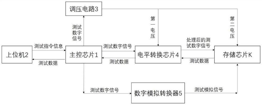
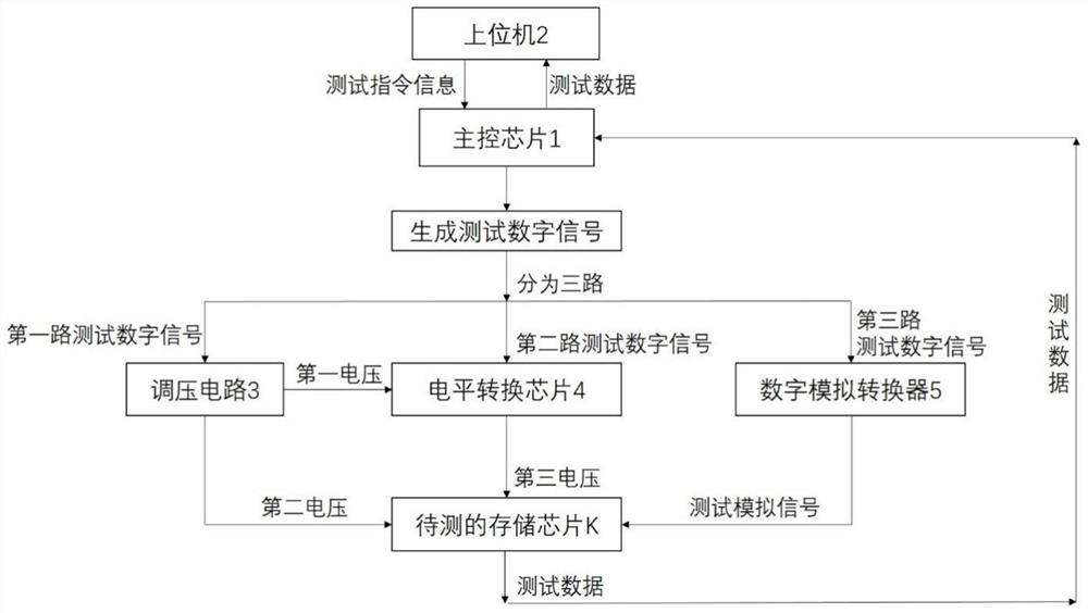
[0032] The present invention provides a write-in depth test system for memory chips. The write-in depth test system adopts a highly integrated board-level design. In this embodiment, the write-in depth test system has a size of 15cm×10cm; Such as figure 1 As shown, it includes: a main control chip 1 , a host computer 2 , a voltage regulating circuit 3 , a level conversion chip 4 and a digital-to-analog converter (DAC) 5 .

[0033] Wherein, the tester inputs the test instruction information of the writing depth test in real time through the host computer 2; Instruction information to generate test digital signals.

[0034] The input terminal of the voltage regulating circuit 3 is connected with t...


PUM


Abstract

The invention discloses a write depth test system for a memory chip, and the system comprises a voltage regulating circuit, wherein the input end of which is connected with the first output end of a main control chip, the first output end of which is connected with the first input end of a level conversion chip, the second output end of which is connected with the first input end of the memory chip to be tested, the second input end of the level conversion chip is connected with the second output end of the main control chip, the first output end of the level conversion chip is connected withthe second input end of the storage chip, and the third input end of the level conversion chip is connected with the output end of the storage chip; and a digital-to-analog converter, wherein the input end of the digital-to-analog converter is connected with the third output end of the main control chip, and the output end of the digital-to-analog converter is connected with the third input end ofthe storage chip. According to the invention, the problems that the traditional ATE cannot be operated off line and is poor in convenience are solved, the VT board level test in an off-line state isrealized by adopting dual power supplies and a high-precision DAC, the test cost is reduced, the test operation is convenient, and the flexible application of various application occasions is satisfied.

Description

technical field [0001] The invention relates to the technical field of chip testing, in particular to a writing depth testing system and method for memory chips. Background technique [0002] For the FLASH memory chip and EEPROM memory chip developed by Puya Semiconductor (PUYA), the traditional writing depth (VT margin) test requires the use of an integrated circuit automatic tester (ATE) machine. [0003] When testing the writing depth test of the FLASH memory chip and EEPROM memory chip developed by PUYA, in addition to completing the laboratory test, it also needs to be tested at the test factory and the field technical support engineer (FAE). However, at present, a dedicated ATE machine is required, which is expensive, bulky, inconvenient, not easy to carry, and cannot be operated offline, which cannot meet the application requirements such as on-site. Contents of the invention [0004] The object of the present invention is to provide a writing depth test system and...

Claims


Application Information

Patent Timeline
Patent Type & Authority Applications(China)
IPC IPC(8): G11C29/56
CPCG11C29/56
Inventor 刘松强钱杨朱庆芳
Owner PUYA SEMICON SHANGHAI CO LTD
Why Eureka
Eureka Blog
Learn More