
Method and appts. for access complex vector located in DSP memory

A vector and complex number technology, applied in the field of processor storage addressing and storage address generation, can solve problems such as difficult memory relocation and low memory application efficiency

Inactive Publication Date: 2003-10-29
INFINEON TECH AG
View PDF1 Cites 0 Cited by
  • Summary
  • Abstract
  • Description
  • Claims
  • Application Information

AI Technical Summary

Problems solved by technology

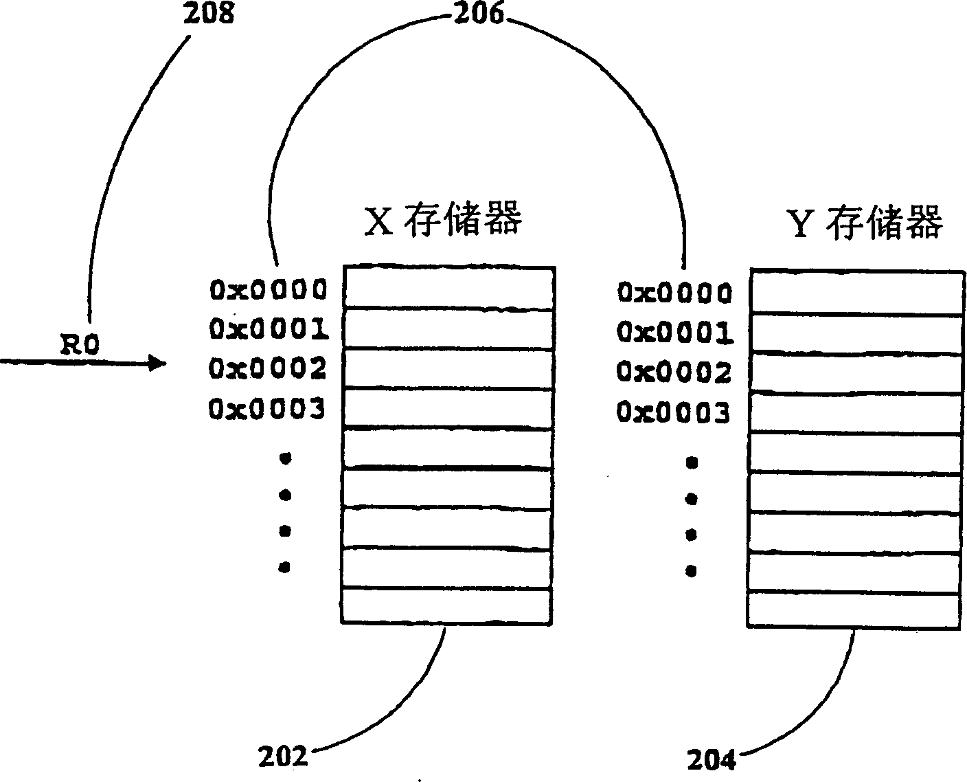
[0013] This solution has two problems: First, the two parts of the vector (pointing to the first array and the second array respectively), must be located in the same location in different memory
This can lead to inefficient use of memory (gaps in memory), while making it difficult to accomplish memory relocation when needed

Method used


Image

  • Method and appts. for access complex vector located in DSP memory
  • Method and appts. for access complex vector located in DSP memory
  • Method and appts. for access complex vector located in DSP memory

Examples


Embodiment Construction

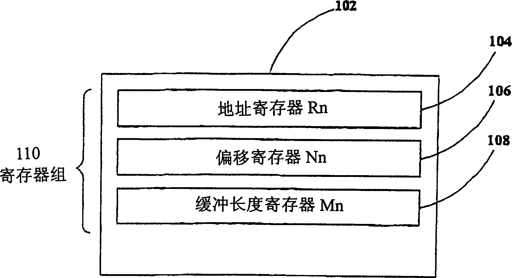
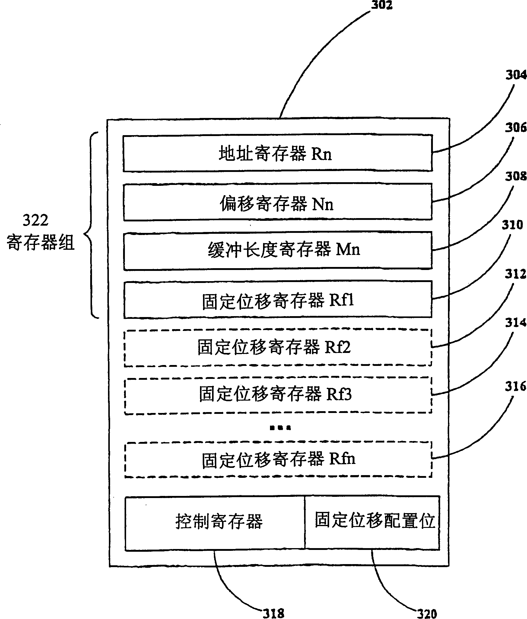
[0026] The principle and operation of a method and device according to the present invention can be explained with the accompanying drawings and corresponding descriptions, and the important part of the device address generating unit of the present invention is shown in image 3 In, the steps of the method of the present invention are in Figure 4 They are illustrated in the flowcharts of , which are implemented in a digital signal processor or other processor according to the invention. These steps implement the fixed displacement mode, which is a new processor mode according to the invention.

[0027] as in image 3 As explained, it is first necessary to provide certain additional hardware capabilities. In particular, the processor must have a fixed shift register 310 in the address generation unit 302, denoted by Rf1. The fixed shift register should be software programmable like all other registers in address generation unit 302 . It is also possible, but not required, to...


PUM


Abstract

A method and apparatus for efficiently accessing the real parts and the imaginary parts of complex vector components in a digital signal processor memory is implemented through the incorporation of a new processor addressing, the fixed displacement mode. An additional register, the fixed displacement register, and an additional control flag, the fixed displacement configuration bit are needed. The method of employment requires only a single address register, and does not require use of the normal offset register used for indexed addressing, leaving the offset register to be used for simultaneous post modification and / or bit reversal. Dual memory spaces sharing a common address space are not required, thereby simplifying memory management, and the method and apparatus are compatible with all addressing.

Description

technical field [0001] The invention relates to a method for processor storage addressing and storage address generation, in particular to a method for accessing complex vectors stored in a digital signal processor memory. Background technique [0002] In US 4 809 156 a circuit for generating memory addresses in a computer system is described. An address generating logic includes two multiplexers (Multiplexer) and an adder, and the adder is connected with the memory address register for outputting the memory address to the central processing unit. Alternative inputs to a multiplexer are from the shift register (Displacement Register) and the extension register. Switching between the two registers is controlled by a sign bit, which is generated by a comparator, and the input value of the comparator is stored in the accumulator and the base address register. The comparator produces a sign detect output signal which reflects the value of the sign flag stored in the flags regi...

Claims


Application Information

Patent Timeline
Patent Type & Authority Patents(China)
IPC IPC(8): G06F9/345G06F9/355G06F9/34G06F12/00G06F12/02G06F17/16
CPCG06F9/345G06F9/3004G06F9/30101G06F9/35G06F12/0646
Inventor 吉尔·纳韦埃兰·魏因加滕
Owner INFINEON TECH AG
Learn More