Substrate processing method and substrate processed by method

A processing method and substrate technology, applied in the direction of metal processing equipment, manufacturing tools, coatings, etc., can solve the problems of changing the atomic distance of the substrate, large mechanical stress, and waste of substrate materials, so as to reduce stress distribution and reduce mechanical stress. The process of processing and the effect of improving quality

Pending Publication Date: 2021-04-09
FUJIAN JING AN OPTOELECTRONICS CO LTD
View PDF7 Cites 1 Cited by
  • Summary
  • Abstract
  • Description
  • Claims
  • Application Information

AI Technical Summary

Problems solved by technology

[0003] In traditional mechanical processing, there is inevitably pressure contact or friction process, which will cause damage on the surface or inside of the substrate, resulting in non-uniform stress on the substrate. Non-uniform stress will have two negative effects: ( 1) Non-uniform stress will change the atomic spacing of the substrate, reduce the quality of epitaxial materials, and increase the defect density; (2) Non-uniform stress will cause deformation of the substrate, resulting in large warpage, such as wire cutting The warp can reach more than 40um
In addition, in traditional mechanical processing, there will be wire cut marks on the surface of the wire slice obtained after wire cutting, and the height is generally 1um to 100um. This is because the diamond wire used for wire cutting has a certain diameter, about 100um to 500um. During the process, the high-speed reciprocating movement of the diamond wire will inevitably cause jitter, and therefore, a wire cut mark will be formed on the surface of the substrate
The appearance of line cut marks may have an impact on the subsequent processing of the substrate
To remove the line cut marks, it is roughly necessary to polish or grind to remove the thickness of 100um, so that the roughness is reduced to below 0.5um. This kind of polishing or grinding to remove the thickness of 100um is a waste of substrate material, which greatly increases the cost of substrate processing. High; in addition, the time required for polishing treatment is too long, such as the current Al 2 o 3 The removal rate of substrate polishing is about 10um / h, that is to say Al 2 o 3 It takes more than 10h to remove 100um thickness, which is obviously not feasible
Furthermore, the mechanical processing method of polishing or grinding for a long time will generate large and non-uniform mechanical stress on the substrate itself, thereby reducing the quality of the substrate.

Method used


Image

  • Substrate processing method and substrate processed by method
  • Substrate processing method and substrate processed by method
  • Substrate processing method and substrate processed by method

Examples


Embodiment Construction

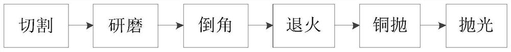
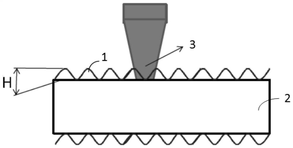
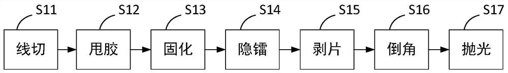
[0043] In order to make the object, technical solution and advantages of the present invention clearer, the present invention will be described in further detail below in conjunction with the embodiments and accompanying drawings. Here, the exemplary embodiments and descriptions of the present invention are used to explain the present invention, but not to limit the present invention.

[0044]Here, it should also be noted that, in order to avoid obscuring the present invention due to unnecessary details, only the structures and / or processing steps closely related to the solution according to the present invention are shown in the drawings, and the related Other details are not relevant to the invention.

[0045] It should be emphasized that the term "comprising / comprising" when used herein refers to the presence of a feature, element, step or component, but does not exclude the presence or addition of one or more other features, elements, steps or components.

[0046] In orde...


PUM

PropertyMeasurementUnit
thicknessaaaaaaaaaa

Abstract

The invention provides a substrate processing method and a substrate processed by the method, and the substrate processing method comprises the following steps: carrying out linear cutting of the substrate, and obtaining a substrate with a preset thickness; carrying out whirl coating treatment on the substrate obtained by cutting to form a layer of flat film on the surface of the substrate; generating a damage layer at a predetermined depth position of the cut substrate by two-dimensionally scanning the cut substrate by a focused laser after the flat film is cured; carrying out stripping processing on the substrate based on the damage layer; and carrying out polishing treatment on the substrate subjected to stripping treatment. According to the substrate processing method and the substrate processed by the method, the machining process can be greatly reduced, so that the stress distribution of the substrate is reduced, the quality of the substrate is improved, and the processing cost of the substrate is reduced.

Description

technical field [0001] The invention relates to the technical field of semiconductor manufacturing, in particular to a substrate processing method and a substrate processed by the method. Background technique [0002] The current conventional substrate processing technology generally includes processes such as wire cutting, grinding, chamfering, annealing, copper polishing and polishing, such as figure 1 As shown, the main processes and mechanisms are mechanical (such as wire cutting, grinding, chamfering and copper polishing), chemical (such as polishing) and thermal processing (such as annealing). [0003] In traditional mechanical processing, there is inevitably pressure contact or friction process, which will cause damage on the surface or inside of the substrate, resulting in non-uniform stress on the substrate. Non-uniform stress will have two negative effects: ( 1) Non-uniform stress will change the atomic spacing of the substrate, reduce the quality of epitaxial mat...

Claims


Application Information

Patent Timeline
Patent Type & Authority Applications(China)
IPC IPC(8): H01L21/268H01L21/428B23K26/53C09D163/10C09D175/14C09D167/06C09D4/06C09D4/02C09D171/02C09D171/08C09D7/63C09D5/20
CPCH01L21/268H01L21/428B23K26/53C09D163/10C09D175/14C09D167/06C09D4/06C09D171/02C09D171/00C09D7/63C09D5/20C08L71/02C08L71/00C08K5/54C08K5/10C08K5/098
Inventor 李瑞评曾柏翔张佳浩杨良
Owner FUJIAN JING AN OPTOELECTRONICS CO LTD
Why Eureka
Try Eureka