Chip packaging structure and packaging method

A technology of chip packaging structure and packaging method, which is applied in the direction of semiconductor/solid-state device parts, semiconductor devices, electrical components, etc., can solve problems such as poor signal performance and poor signal quality, and achieve improved connection reliability and reduced Volume, cost reduction effect

Inactive Publication Date: 2021-04-09
SZ DJI TECH CO LTD
View PDF7 Cites 1 Cited by
  • Summary
  • Abstract
  • Description
  • Claims
  • Application Information

AI Technical Summary

Problems solved by technology

[0003] However, the existing pan / tilt products connected by soft signal lines also have certain defects when in use. For example, when the signal line propagates the signal, sometimes it will cause a certain degree of distortion to key indicators such as the amplitude of the signal, the upper and lower edges, etc. Influence, making the SI (signal integrity) performance of the signal poor, resulting in poor signal quality received by the electronic equipment at the end of the gimbal load

Method used


Image

  • Chip packaging structure and packaging method
  • Chip packaging structure and packaging method
  • Chip packaging structure and packaging method

Examples


Embodiment 1

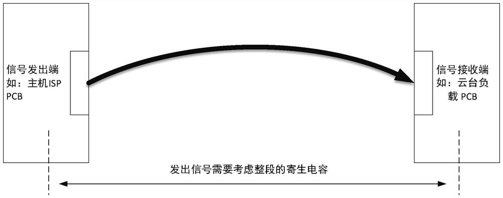
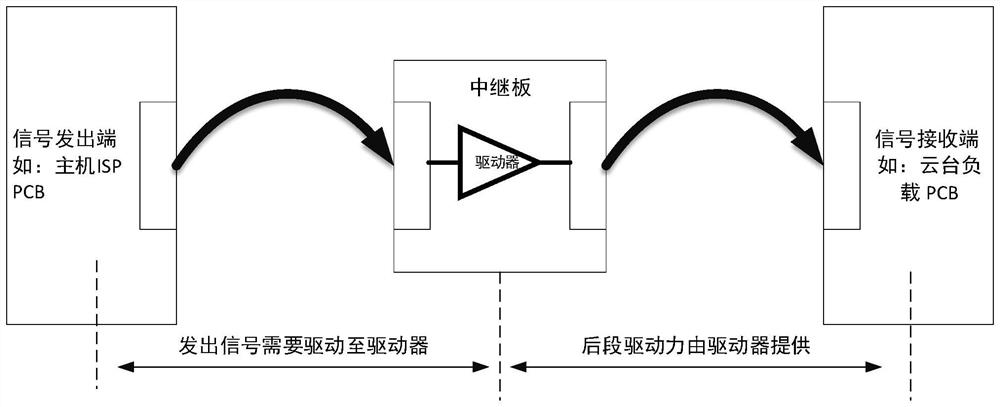
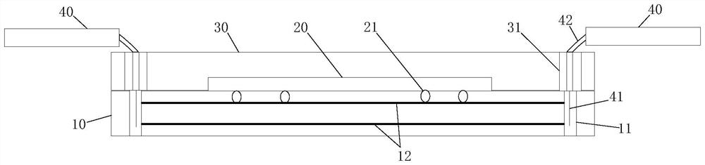
[0071] image 3 It is a structural schematic diagram of a section of a chip package structure in the present invention. Figure 4 It is a structural schematic diagram of the top of the chip package structure in the present invention, wherein the chip 20 is in a see-through state. combine image 3 and Figure 4 shown in .

[0072] In one embodiment of the present invention, a chip packaging structure is provided, including: a substrate 10 , a chip 20 and a protective layer 30 . Wherein, the substrate 10 has a first connection portion and a second connection portion 11 , and the first connection portion and the second connection portion 11 are electrically connected through the internal circuit 13 of the substrate 10 . Wherein, the second connection portion 11 is a through hole penetrating the substrate 10 , and an electroplating layer with a connection hole is disposed in the through hole. The chip 20 is disposed on the substrate 10 and is electrically connected to the fir...

Embodiment 2

[0112] Correspondingly, in one embodiment of the present invention, a packaging method of the chip 20 is also provided, and the method in the second embodiment can manufacture the chip packaging structure described in the first embodiment. The specific plan is as follows:

[0113] see Figure 8 , combined with image 3 and Figure 4 , in one embodiment of the present invention, also provides a kind of packaging method of chip 20, comprise:

[0114] Step S101: disposing the chip 20 on the substrate 10, so that the chip 20 is electrically connected to the first connection part on the substrate 10; wherein, the substrate 10 has a first connection part and a second connection part 11, and the first connection part and the second connection part The two connecting parts 11 are electrically connected through the internal circuit 13 of the substrate 10; wherein, the second connecting part 11 is a through hole penetrating the substrate 10, and an electroplating layer with a connect...


PUM

PropertyMeasurementUnit
lengthaaaaaaaaaa
thicknessaaaaaaaaaa

Abstract

The embodiment of the invention provides a chip packaging structure and packaging method. The structure comprises a substrate which is provided with a first connection part and a second connection part, wherein the first connection part and the second connection part are electrically connected through an internal circuit of the substrate, the second connection part is a through hole penetrating through the substrate, and an electroplated layer with a connecting hole is arranged in the through hole; a chip arranged on the substrate and electrically connected with the first connection part, so that a signal path is formed between the second connection part and the chip through the internal circuit of the substrate; a protective layer which is arranged on the substrate and wraps the chip and the second connection part, wherein a wire passing hole is formed in the position, corresponding to the second connection part, of the protective layer so that the signal wire can penetrate through the wire passing hole to be electrically connected with the second connection part. According to the technical scheme provided by the embodiment of the invention, the parasitic capacitance on the signal path can be reduced, the signal quality of a receiving end is effectively improved, the signal line connection reliability is improved, the size is reduced, and the cost is reduced.

Description

technical field [0001] The embodiments of the present invention relate to the technical field of packaging, and in particular to a chip packaging structure and a packaging method. Background technique [0002] At present, in terms of gimbal product form, due to the mechanical structure of the gimbal, the electronic equipment at the end of the gimbal load and the core motherboard of the fuselage need to be connected through multiple soft signal lines. Compared with FPC (Flexible Printed Circuit, flexible circuit board), the soft signal line has better characteristic impedance continuity and less high-frequency component loss. It is a better way to connect the gimbal side under the condition of insensitive cost. [0003] However, the existing pan / tilt products connected by soft signal lines also have certain defects when in use. For example, when the signal line propagates the signal, sometimes it will cause a certain degree of distortion to key indicators such as the amplitud...

Claims


Application Information

Patent Timeline
Patent Type & Authority Applications(China)
IPC IPC(8): H01L23/498H01L23/485H01L23/482H01L23/31H01L21/56H01L21/60
CPCH01L23/49827H01L23/4824H01L23/485H01L24/81H01L21/56H01L23/3121H01L2224/02331H01L2224/02381H01L2224/0231
Inventor 张鼎王腾飞许美蓉李文浩
Owner SZ DJI TECH CO LTD
Why Eureka
Try Eureka