Gasket and its manufacturing method, package structure and its manufacturing method

A packaging structure and gasket technology, applied in semiconductor/solid-state device manufacturing, semiconductor devices, electrical components, etc., can solve problems such as difficulty, occupy a large space, limit the space of passive components, etc., achieve good electrical performance, save space, The effect of reducing the device

Active Publication Date: 2022-08-09
YANGTZE MEMORY TECH CO LTD
View PDF12 Cites 0 Cited by
  • Summary
  • Abstract
  • Description
  • Claims
  • Application Information

AI Technical Summary

Problems solved by technology

When the package structure includes multiple bare cores, multiple passive components such as resistors and capacitors need to be placed, and these passive components need to occupy a large space
However, the internal space of the packaging structure is limited, which limits the space available for passive components.
[0005] It is very difficult to arrange more passive components, and it is even impossible to realize such a packaging structure
In addition, general-purpose passive components have a plastic package and pin structure, which is a redundant structure that takes up space for the package structure

Method used


Image

  • Gasket and its manufacturing method, package structure and its manufacturing method
  • Gasket and its manufacturing method, package structure and its manufacturing method
  • Gasket and its manufacturing method, package structure and its manufacturing method

Examples


Embodiment Construction

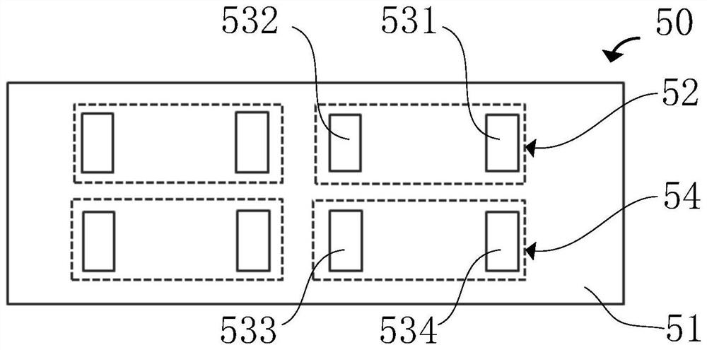
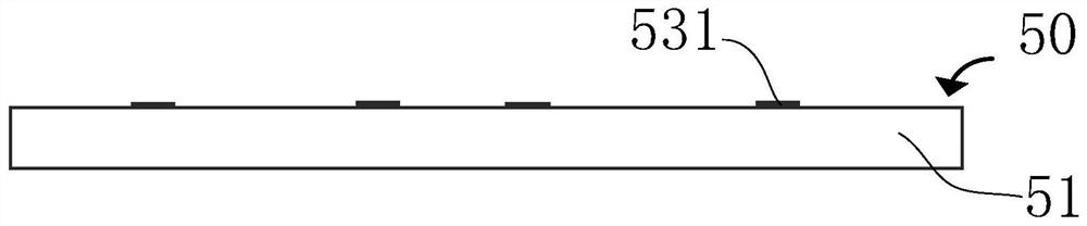
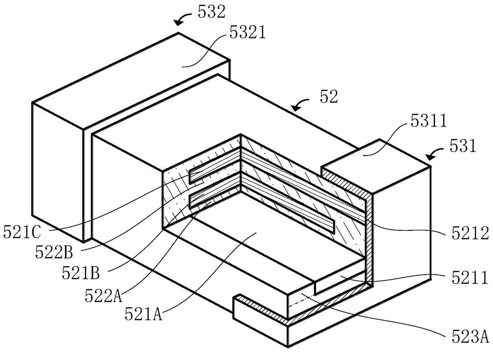
[0071] For a better understanding of the present application, various aspects of the present application will be described in more detail with reference to the accompanying drawings. It should be understood that these detailed descriptions are merely illustrative of exemplary embodiments of the present application and are not intended to limit the scope of the present application in any way. Throughout the specification, the same reference numerals refer to the same elements. The expression "and / or" includes any and all combinations of one or more of the associated listed items.

[0072] It should be noted that in this specification, the expressions first, second, third etc. are only used to distinguish one feature from another feature and do not imply any limitation on the feature. Accordingly, the first electrode discussed below may also be referred to as a second electrode without departing from the teachings of the present application. vice versa.

[0073] In the drawin...


PUM


Abstract

The present application provides a gasket and a manufacturing method thereof, a packaging structure and a manufacturing method thereof. The spacer includes: a base plate; at least one passive element structure is formed at a first surface of the base plate and includes a circuit pattern formed by a planar process, the circuit pattern including at least two functional terminals for electrical connection with an external circuit; and At least two electrodes are formed on the functional end of the passive element structure, and are used to electrically connect the functional end and the external circuit.

Description

technical field [0001] The present application relates to the field of semiconductor devices, and more particularly, to a gasket, a method for manufacturing a gasket, a package structure, and a method for manufacturing a package structure. Background technique [0002] With the continuous development of the microelectronics industry, the integration of semiconductor devices is getting higher and higher. Semiconductor memory has also developed from two-dimensional to three-dimensional, such as three-dimensional NAND flash (3D NAND flash). And flash memory is constantly being upgraded. [0003] At present, when designing a system-level packaging structure of a memory, in order to improve the signal integrity and power integrity of the memory, some passive components are usually arranged on the bottom plate in the packaging structure. For example, high precision (eg 1%) resistors are placed on the backplane to calibrate the drive impedance and termination resistors, and capac...

Claims


Application Information

Patent Timeline
Patent Type & Authority Patents(China)
IPC IPC(8): H01L27/06H01L27/08H01L21/822H01L27/11524H01L27/11551H01L27/1157H01L27/11578
CPCH01L27/06H01L27/0802H01L27/0805H01L21/822H10B41/20H10B41/35H10B43/20H10B43/35
Inventor 曾心如陈鹏王利琴周厚德侯春源
Owner YANGTZE MEMORY TECH CO LTD
Why Eureka
Try Eureka