
Ultra-wideband bidirectional amplifier based on 500nm GaAs pHEMT process

A bidirectional amplifier and ultra-wideband technology, which is applied to bidirectional amplifiers, amplifiers, improved amplifiers to improve efficiency, etc., can solve problems such as low process cut-off frequency, difficulties in ultra-wideband, difficulties in bidirectional amplifier chips, etc., and achieve the effect of convenient use

Active Publication Date: 2021-04-13
UNIV OF ELECTRONICS SCI & TECH OF CHINA
View PDF12 Cites 4 Cited by
  • Summary
  • Abstract
  • Description
  • Claims
  • Application Information

AI Technical Summary

Problems solved by technology

Although the cost of the 500nm GaAs pHEMT process is low, the cut-off frequency of this process is low. It will be very difficult to design a bidirectional amplifier chip that achieves high frequency coverage. It will be even more difficult to achieve ultra-wideband while covering high frequency

Method used


Image

  • Ultra-wideband bidirectional amplifier based on 500nm GaAs pHEMT process
  • Ultra-wideband bidirectional amplifier based on 500nm GaAs pHEMT process
  • Ultra-wideband bidirectional amplifier based on 500nm GaAs pHEMT process

Examples


Embodiment 1

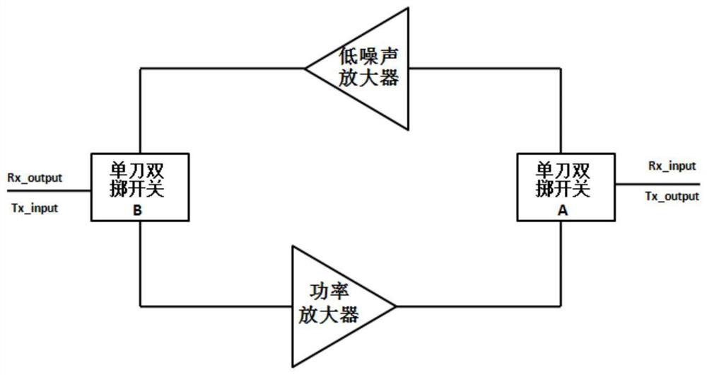
[0032] Such as figure 1 As shown, an ultra-broadband bidirectional amplifier based on 500nm GaAs pHEMT process, including low noise amplifier, power amplifier, SPDT switch A and SPDT switch B.

[0033] Among them, the low-noise amplifier is used to realize wide-band and low-noise matching, and the power amplifier is used to realize wide-band and maximum power matching. When the single-pole double-throw switch A is connected to the input terminal Rx_input of the low-noise amplifier, and when the single-pole double-throw switch B is connected to the output terminal Rx_output of the low-noise amplifier, the current signal is input from the input terminal Rx_input and enters the low-noise amplifier through the single-pole double-throw switch A , after widening the frequency band and reducing noise, it is output from the output terminal Rx_output; when the single-pole double-throw switch B is connected to the input terminal Tx_input of the power amplifier, and the single-pole doubl...

Embodiment 2

[0045] Such as Figure 7 As shown, the positive pressure control switch unit includes two identical switch circuits and one external power supply a. Wherein, the switch circuit includes a first transistor, a second transistor, a power supply Vcnt1, a power supply Vcnt2, a first power supply, a second power supply, a first resistor, a second resistor, a third resistor, a fourth resistor and a capacitor; the source of the first transistor One end of the first resistor is connected to the gate of the first transistor, and the other end is connected to the power supply Vcnt1; one end of the second resistor is connected to the first power supply, and the other end is connected between the source of the first common transistor and the bidirectional amplifier ; The source of the second transistor is connected to the ground after the first capacitor, and the drain is connected between the second resistor and the bidirectional amplifier; one end of the third resistor is connected to th...


PUM


Abstract

The invention discloses an ultra-wideband bidirectional amplifier based on a 500nm GaAs pHEMT process, which comprises a low-noise amplifier for realizing wideband and low-noise matching, a power amplifier for realizing wideband and maximum power matching, a single-pole double-throw switch A and a single-pole double-throw switch B, and two ends of a switch tube of the ultra-wideband bidirectional amplifier are respectively provided with the same 5V positive voltage control switch unit. The ultra-wideband bidirectional amplifier based on the 500nm GaAs pHEMT process can realize ultra-wideband and high-frequency coverage to 10.6 GHz at the same time, and has excellent performance of an Rx-path LNA amplifier and a Tx-path PA amplifier. In addition, the 5V positive pressure control switch units arranged at the two ends change a negative pressure control switch tube into positive pressure control, and use is more convenient.

Description

technical field [0001] The invention relates to the technical field of bidirectional amplifiers, in particular to an ultra-wideband bidirectional amplifier based on a 500nm GaAs pHEMT process. Background technique [0002] Driven by the continuous advancement of semiconductor material epitaxy technology, chip integrated circuits have also developed rapidly in recent years. Silicon (Si), silicon germanium (SiGe), gallium arsenide (GaAs) and other materials are often used in chip production, and traditional amplifiers are generally produced based on Si-based CMOS technology. However, low-noise amplifiers, power amplifiers and other common components in transceiver systems based on Si-based CMOS technology have insufficient performance in terms of noise and power. Research on amplifier chips based on GaAs pHEMT technology has become the focus, which has promoted the application of amplifiers in ultra-wideband systems. Although the cost of the 500nm GaAs pHEMT process is low, ...

Claims


Application Information

Patent Timeline
IPC IPC(8): H03F1/02H03F3/62
CPCH03F1/0211H03F3/62Y02D30/70
Inventor 马凯学李一夫
Owner UNIV OF ELECTRONICS SCI & TECH OF CHINA
Learn More