Bonding method for preventing injection molding deformation of long-span bonding lead of integrated circuit

A technology of bonding wires and integrated circuits, applied in circuits, electrical components, electric solid devices, etc., can solve the problems of many pins, small spacing, long-span bonding wire arc injection deformation, etc.

Pending Publication Date: 2021-04-20
GUIZHOU ZHENHUA FENGGUANG SEMICON
View PDF0 Cites 0 Cited by
  • Summary
  • Abstract
  • Description
  • Claims
  • Application Information

AI Technical Summary

Problems solved by technology

[0004] The purpose of the present invention is to solve the problem of how to prevent long-span bonding wire arc injection moldi

Method used


Image

  • Bonding method for preventing injection molding deformation of long-span bonding lead of integrated circuit
  • Bonding method for preventing injection molding deformation of long-span bonding lead of integrated circuit
  • Bonding method for preventing injection molding deformation of long-span bonding lead of integrated circuit

Examples


Embodiment Construction

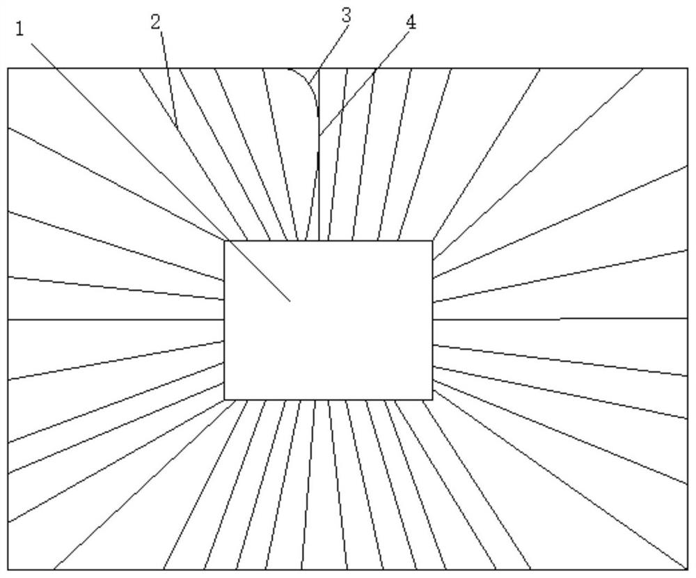
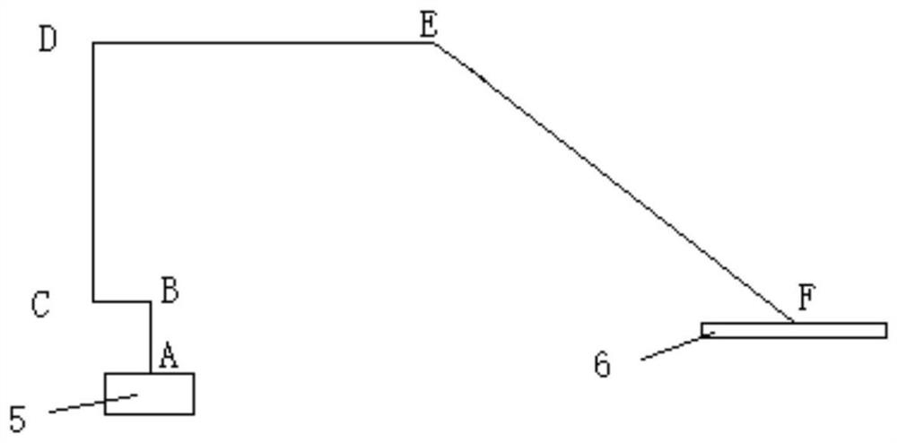
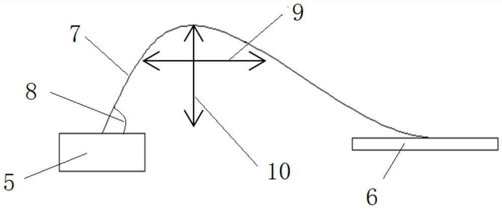
[0036] Taking the LQFP100 type plastic package product as an example, a φ20μm gold wire is used, and the bonding distance is between 3mm and 5mm. The bonding equipment used is ASM’s iHawk Xtreme GoCu. The conventional bonding wire arc height is generally set at 150 μm to 200 μm, and the inclination angle is generally set at 90°. When the bonding distance (AF) is greater than 3mm, use the original The shape of the arc parameters cannot avoid the problem of the offset of the bonding wire in the middle part. The schematic diagram of the conventional arc path is as follows figure 2 , image 3 shown.

[0037] According to the bonding method of the present invention, in order to avoid the offset of the bonding wire during the injection molding process, a new bonding wire arc structure is designed. As shown in Table 1:

[0038] Table 1 Long-distance bonding wire arc parameter test factor level table

[0039]

[0040] in:

[0041] 1. Height of broken line (AB): the distance f...


PUM

PropertyMeasurementUnit
Wire diameteraaaaaaaaaa

Abstract

The invention discloses a bonding method for preventing injection molding deformation of a long-span bonding lead of an integrated circuit, and the method comprises the following steps: enabling a set gold wire to penetrate into a hole at the top of a chopper, and to penetrate out of a port at the bottom of the chopper; enabling the chopper port to drive the bonding wire to be bonded at the first bonding point A; enabling the port of the chopper to rise backwards to a set height point B according to a set inclination angle; translating the port of the chopper backwards to a set distance C point; vertically lifting the chopper port to a set height D point; moving the port of the chopper to a point E forwards and upwards according to a set height and a set distance; and moving the chopper port forwards and downwards to a second bonding point F to finish bonding and finish lead bonding between the first bonding point A and the second bonding point F. The problem that in an existing plastic packaging technology, under the conditions that the number of pins is large, the distance is small, gold wires are thin, and the span is long, a long-span bonding wire arc is deformed through injection molding is solved. And the method can be popularized to similar long-span lead wire key products according to the wire diameter of the gold wire.

Description

technical field [0001] The present invention relates to the field of semiconductor chip packaging, more specifically, to the field of semiconductor chip plastic packaging, and specifically to the technical field of plastic packaging chip wire bonding. Background technique [0002] In the semiconductor industry, in order to realize the electrical connection between the chip circuit and the casing leads, it is necessary to use a bonding wire (usually gold wire, silicon aluminum wire or copper wire) to connect the electrode output point (chip bonding point) on the chip with the package The corresponding pin bonding points of the shell are connected together. Especially for plastic-encapsulated semiconductor integrated circuits, considering the requirements of packaging reliability, packaging cost, large-scale scale and automatic production, thinner gold wires are usually used as bonding wires to connect wires between electrode bonding points. When the wire is bonded and connec...

Claims


Application Information

Patent Timeline
IPC IPC(8): H01L23/49
CPCH01L2224/4809H01L2224/48247H01L2224/85181
Inventor 李阳周恒谌帅业聂平健商登辉
Owner GUIZHOU ZHENHUA FENGGUANG SEMICON
Why Eureka
Try Eureka