Preparation process of long-life diode
A preparation process and diode technology, which is applied in semiconductor/solid-state device manufacturing, electrical components, circuits, etc., can solve the problems of difficult concentricity assurance, many pitting, and unclean cleaning.
- Summary
- Abstract
- Description
- Claims
- Application Information
AI Technical Summary
Problems solved by technology
Method used
Image

Examples
Embodiment 1
[0061] Example 1. A preparation process for a long-life diode, characterized in that:
[0062] Including the following steps:
[0063] Step 1: Preparation of Diode Die
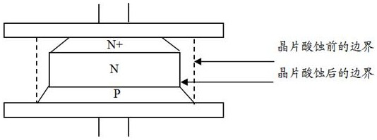
[0064] 1.1: Pre-cut in the thickness direction of the silicon wafer to form incompletely cut diode grains, and the cutting depth of the silicon wafer is 2 / of the total thickness of the silicon wafer.
[0065] 1.2: Put the pre-cut silicon wafer in the thickness direction N side down on the crystal cracking paper, with the cutting edge facing upward, and press lightly, so that the incompletely cut diode crystal grains are completely cracked to form a wafer.
[0066] Step 2: Rosin Isopropanol Solution Sprayed to Copper Lead Electrodes
[0067] In the rosin isopropanol solution, the mass ratio of rosin to isopropanol is 1:10;
[0068] Step 3: Filling
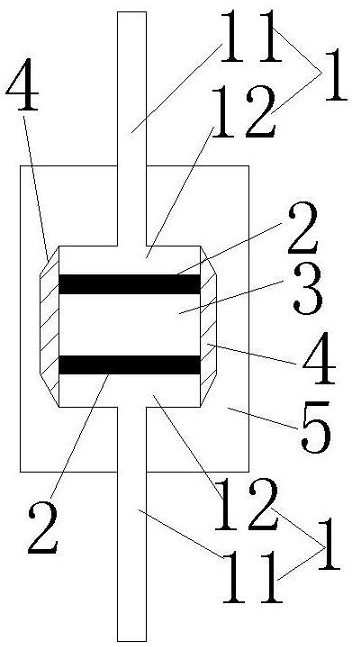
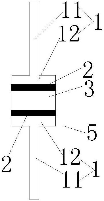
[0069] Put two copper lead electrodes 1, two soldering pieces 2, and chip 3 into the fixture; each copper lead electrode includes a table top 12 and a lead wi...
Embodiment 2
[0090] Example 2. A preparation process for a long-life diode, characterized in that:
[0091] Including the following steps:
[0092] Step 1: Preparation of Diode Die
[0093] 1.1: Pre-cut in the thickness direction of the silicon wafer to form incompletely cut diode grains, and the cutting depth of the silicon wafer is 3 / 4 of the total thickness of the silicon wafer;
[0094] 1.2: Put the pre-cut silicon wafer in the thickness direction N side down on the crystal cracking paper, with the cutting edge facing upward, and press lightly, so that the incompletely cut diode crystal grains are completely cracked to form a wafer.
[0095] Step 2: Rosin Isopropanol Solution Sprayed to Copper Lead Electrodes
[0096] In the rosin isopropanol solution, the mass ratio of rosin to isopropanol is 1:10-15;
[0097] Step 3: Filling
[0098] Put two copper lead electrodes 1, two soldering pieces 2, and chip 3 into the fixture; each copper lead electrode includes a table top 12 and a lea...
Embodiment 3
[0118] Example 3. A preparation process for a long-life diode, characterized in that:
[0119] Including the following steps:
[0120] Step 1: Preparation of Diode Die
[0121] 1.1: Pre-cut in the thickness direction of the silicon wafer to form incompletely cut diode grains, and the cutting depth of the silicon wafer is 2 / 3 of the total thickness of the silicon wafer;
[0122] 1.2: Put the pre-cut silicon wafer in the thickness direction N side down on the crystal cracking paper, with the cutting edge facing upward, and press lightly, so that the incompletely cut diode crystal grains are completely cracked to form a wafer.
[0123] Step 2: Rosin Isopropanol Solution Sprayed to Copper Lead Electrodes
[0124] In the rosin isopropanol solution, the mass ratio of rosin to isopropanol is 1:12;
[0125] Step 3: Filling
[0126]Put two copper lead electrodes 1, two soldering pieces 2, and chip 3 into the fixture; each copper lead electrode includes a table top 12 and a lead wi...
PUM
| Property | Measurement | Unit |
|---|---|---|
| Thickness | aaaaa | aaaaa |
| Diameter | aaaaa | aaaaa |
| Thickness | aaaaa | aaaaa |
Abstract
Description
Claims
Application Information
PatSnap Eureka turns technology decisions into work you can execute. Powered by our Innovation Knowledge Graph, it runs expert workflows across engineering, life sciences, materials and intellectual property. Get your review-ready output in minutes.


