Manufacturing method of high-stability open-junction plastic package silicon rectifier diode
A silicon rectifier diode, a high-stability technology, applied in semiconductor/solid-state device manufacturing, semiconductor devices, electrical components, etc., can solve problems such as many pits, unclean cleaning, and difficulty in ensuring concentricity, so as to ensure stability , Solve the problem of concentricity and reduce the effect of welding stress
- Summary
- Abstract
- Description
- Claims
- Application Information
AI Technical Summary
Problems solved by technology
Method used
Image

Examples
Embodiment 1
[0064] Example 1. A method for manufacturing a highly stable open junction plastic-sealed silicon rectifier diode, comprising the steps of:
[0065] Step 1: Preparation of Diode Die
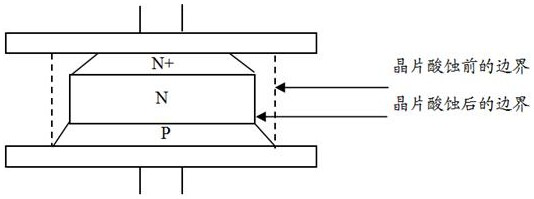
[0066] 1.1: Pre-cut in the thickness direction of the silicon wafer to form incompletely cut diode grains, and the cutting depth of the silicon wafer is 2 / of the total thickness of the silicon wafer.
[0067] 1.2: Put the pre-cut silicon wafer in the thickness direction N side down on the crystal cracking paper, with the cutting edge facing upward, and press lightly, so that the incompletely cut diode crystal grains are completely cracked to form a wafer.
[0068] Step 2: Tempering of Copper Lead Electrodes
[0069] Put the two copper lead electrodes into the welding boat and put them into the tunnel furnace for tempering;
[0070] There are five protective gas nozzles of the tunnel furnace, the first nozzle is set at the feed port of the tunnel furnace, the fifth nozzle is set at the dischar...
Embodiment 2
[0096] Example 2. A method for manufacturing a high-stability open-junction plastic-sealed silicon rectifier diode, characterized in that:
[0097] Including the following steps:
[0098] Step 1: Preparation of Diode Die
[0099] 1.1: Pre-cut in the thickness direction of the silicon wafer to form incompletely cut diode grains, and the cutting depth of the silicon wafer is 3 / 4 of the total thickness of the silicon wafer;
[0100] 1.2: Put the pre-cut silicon wafer in the thickness direction N side down on the crystal cracking paper, with the cutting edge facing upward, and press lightly, so that the incompletely cut diode crystal grains are completely cracked to form a wafer.
[0101] Step 2: Tempering of Copper Lead Electrodes
[0102] Put the two copper lead electrodes into the welding boat and put them into the tunnel furnace for tempering;
[0103] There are five protective gas nozzles of the tunnel furnace, the first nozzle is set at the feed port of the tunnel furnac...
Embodiment 3
[0128] Example 3. A method for manufacturing a highly stable open junction plastic-sealed silicon rectifier diode, comprising the steps of:
[0129] Step 1: Preparation of Diode Die
[0130] 1.1: Pre-cut in the thickness direction of the silicon wafer to form incompletely cut diode grains, and the cutting depth of the silicon wafer is 2 / 3 of the total thickness of the silicon wafer;
[0131] 1.2: Put the pre-cut silicon wafer in the thickness direction N side down on the crystal cracking paper, with the cutting edge facing upward, and press lightly, so that the incompletely cut diode crystal grains are completely cracked to form a wafer.
[0132] Step 2: Tempering of Copper Lead Electrodes
[0133] Put the two copper lead electrodes into the welding boat and put them into the tunnel furnace for tempering;
[0134] There are five protective gas nozzles of the tunnel furnace, the first nozzle is set at the feed port of the tunnel furnace, the fifth nozzle is set at the discha...
PUM
| Property | Measurement | Unit |
|---|---|---|
| Thickness | aaaaa | aaaaa |
| Diameter | aaaaa | aaaaa |
| Thickness | aaaaa | aaaaa |
Abstract
Description
Claims
Application Information
PatSnap Eureka turns technology decisions into work you can execute. Powered by our Innovation Knowledge Graph, it runs expert workflows across engineering, life sciences, materials and intellectual property. Get your review-ready output in minutes.


