A multi -chip module

A multi-chip module and multi-layer circuit board technology, which is applied in semiconductor/solid-state device components, semiconductor devices, electrical components, etc., can solve problems such as inability to realize MCM circuit functions, affect the convenience of MCM application, and difficult internal device parameters. , to achieve the effect of reducing the quantity, reducing the influence of electrical performance, and reducing the difficulty of debugging

Active Publication Date: 2022-08-09
DYNAX SEMICON
View PDF5 Cites 0 Cited by
  • Summary
  • Abstract
  • Description
  • Claims
  • Application Information

AI Technical Summary

Problems solved by technology

[0003] The traditional MCM uses an integrated passive device (Integrated Passive Device, IPD) to form the required circuit function. Once the IPD is manufactured, its internal device parameters are difficult to modify, which makes the overall circuit debugging less flexible. , it may not be possible to realize all the circuit functions of the MCM. At this time, additional circuits need to be added off-chip, which affects the convenience of MCM applications.

Method used


Image

  • A multi -chip module
  • A multi -chip module
  • A multi -chip module

Examples


Embodiment Construction

[0028] The present invention will be further described in detail below in conjunction with the accompanying drawings and embodiments. It should be understood that the specific embodiments described herein are only used to explain the present invention, but not to limit the present invention. In addition, it should be noted that, for the convenience of description, the drawings only show some but not all structures related to the present invention. Throughout this specification, the same or similar reference numbers represent the same or similar structures, elements or processes. It should be noted that the embodiments in the present application and the features of the embodiments may be combined with each other in the case of no conflict.

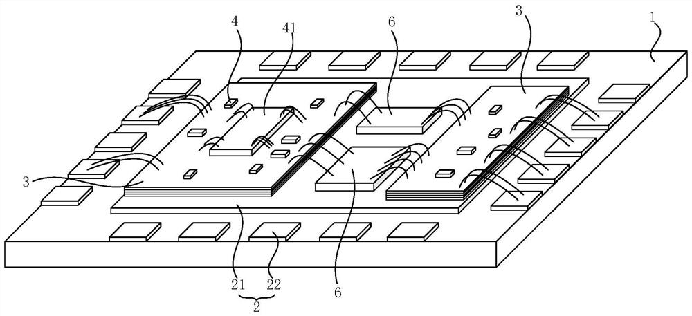
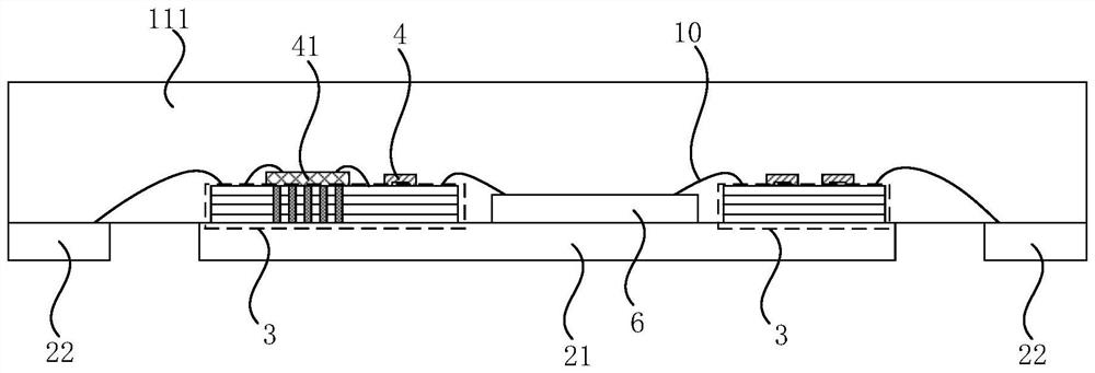
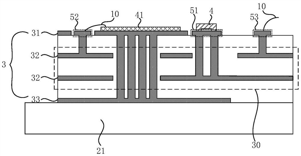
[0029] An embodiment of the present invention provides a multi-chip module, the multi-chip module includes a base and a lead frame on the base, the multi-chip module further includes at least one multi-layer circuit board mounted on the le...


PUM


Abstract

A multi-chip module, the multi-chip module includes a base and a lead frame located on the base, the multi-chip module further includes at least one multi-layer circuit board mounted on the lead frame, and the multi-layer circuit board includes at least three wiring layers, The top layer of the multi-layer circuit board is surface-mounted with a plurality of independent passive devices, and the top layer of at least one multi-layer circuit board is bonded with integrated passive devices. Through the technical scheme of the present invention, the difficulty of debugging the multi-chip module is reduced, the number of bonding wires used for setting passive devices in the multi-chip module is reduced, and the plastic-encapsulated key used in packaging the multi-chip module is reduced. The effect of the alignment.

Description

technical field [0001] Embodiments of the present invention relate to the field of chips, and in particular, to a multi-chip module. Background technique [0002] A Multichip Module (MCM) places multiple unpackaged integrated circuits (ICs) or semiconductor dies and other discrete components on a unified substrate, which can be viewed as a single component when used. Compared with the solution in which each IC is individually packaged, MCM saves raw materials, reduces the manufacturing process, and greatly reduces the occupied area. Compared with the traditional discrete solution, the MCM solution has a higher degree of integration and can save more area costs. Therefore, has been widely used. [0003] The traditional MCM uses Integrated Passive Device (IPD) to form the required circuit functions. Once the IPD is fabricated, its internal device parameters are difficult to modify, making the overall circuit debugging less flexible, and due to the limitations of the IPD devic...

Claims


Application Information

Patent Timeline
Patent Type & Authority Patents(China)
IPC IPC(8): H01L23/495H01L25/16
CPCH01L23/49575H01L23/49527H01L23/49531H01L25/16H01L23/49568H01L2224/48227H01L2924/19107H01L2224/48091H01L2924/181H01L2924/00014H01L2924/00012
Inventor 刘鑫赵洋阎述昱
Owner DYNAX SEMICON
Why Eureka
Try Eureka