Display panel, preparation method and display device

A display panel and sub-panel technology, which is applied to electrical components, electrical solid devices, circuits, etc., can solve problems affecting the normal light emission of micro light-emitting diodes, achieve the effects of saving production costs, simplifying process steps, and improving light extraction efficiency

Active Publication Date: 2021-05-11
XIAMEN TIANMA MICRO ELECTRONICS
View PDF8 Cites 4 Cited by
  • Summary
  • Abstract
  • Description
  • Claims
  • Application Information

AI Technical Summary

Problems solved by technology

[0004] In view of this, the embodiment of the present invention provides a display panel, a manufacturing method and a display device to solve the problem of the preparation process and / or The height setting will have a new impact on the micro-LEDs, which in turn will affect the normal lighting of the micro-LEDs

Method used


Image

  • Display panel, preparation method and display device
  • Display panel, preparation method and display device
  • Display panel, preparation method and display device

Examples


preparation example Construction

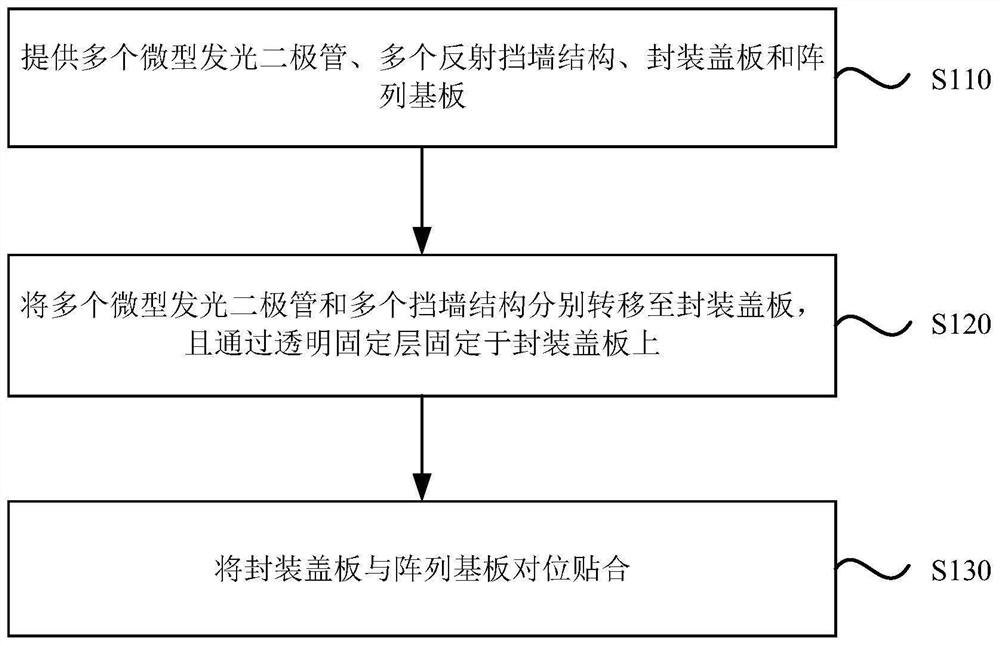
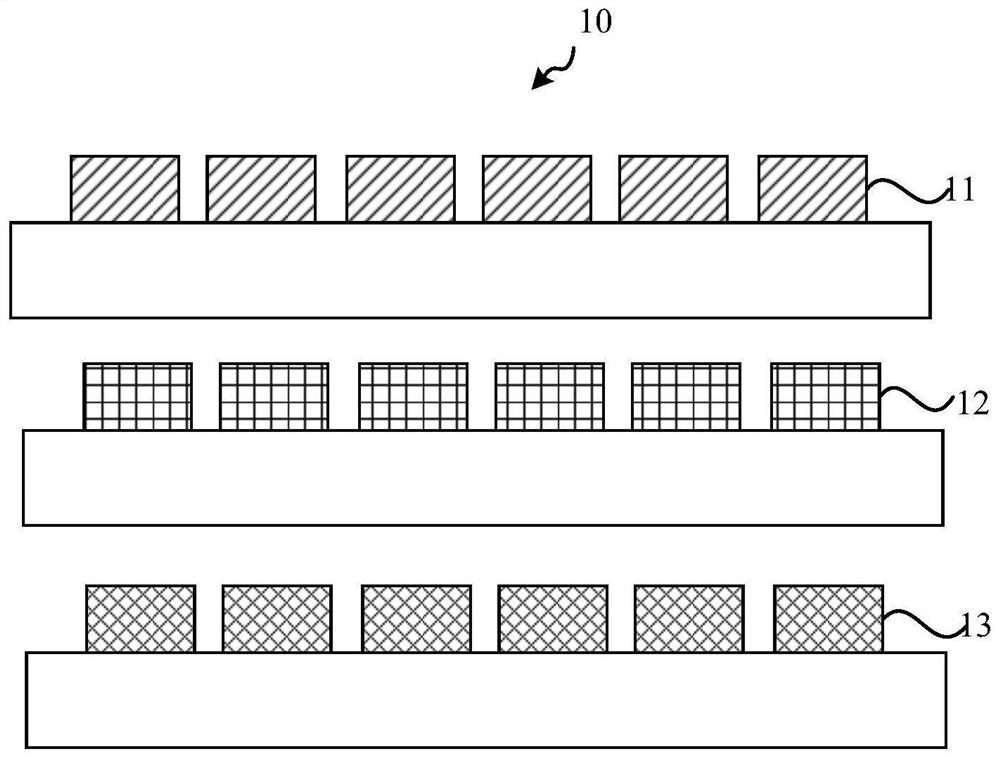
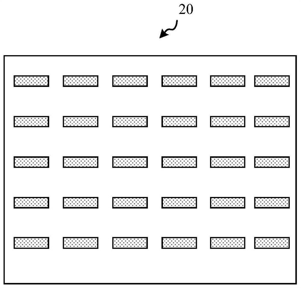
[0051]In view of the problems of the background technology, an embodiment of the present invention provides a method for manufacturing a display panel. The method for manufacturing a display panel includes: providing a plurality of miniature light-emitting diodes, a plurality of reflective wall structures, a packaging cover plate, and an array substrate; The packaging cover plate includes a cover plate and a transparent fixed layer on one side of the cover plate; the array substrate includes a base substrate and a conductive layer on one side of the base substrate; the conductive layer includes a plurality of conductive electrodes; multiple micro light emitting diodes and multiple The reflective wall structures are respectively transferred to the package cover plate, and fixed on the package cover plate through a transparent fixing layer; at least one micro light-emitting diode forms a pixel unit; the reflective wall structure is located between adjacent pixel units; the package...


PUM


Abstract

The embodiment of the invention discloses a display panel, a preparation method and a display device. The preparation method comprises following steps: providing a plurality of micro light-emitting diodes, a plurality of reflection retaining wall structures, a packaging cover plate and an array substrate, wherein the packaging cover plate comprises a cover plate and a transparent fixing layer located on one side of the cover plate; the array substrate comprises a substrate body and a conductive layer located on one side of the substrate body; and the conductive layer comprises a plurality of conductive electrodes; respectively transferring the plurality of micro light-emitting diodes and the plurality of reflection retaining wall structures to the packaging cover plate, and fixing the micro light-emitting diodes and the reflection retaining wall structures on the packaging cover plate through a transparent fixing layer, wherein at least one micro light emitting diode forms a pixel unit and the reflection retaining wall structures are located between the adjacent pixel units; attaching the packaging cover plate and the array substrate in an aligned mode, wherein the attaching mode is that the side, provided with the micro light-emitting diodes, of the packaging cover plate is attached to the conductive layer of the array substrate in an aligned mode, the conductive electrodes are electrically connected with the micro light-emitting diodes in a one-to-one correspondence mode, and the cover plate is reused as a packaging layer of the display panel.

Description

technical field [0001] Embodiments of the present invention relate to the field of display technology, and in particular, to a display panel, a manufacturing method, and a display device. Background technique [0002] At present, Micro Light Emitting Diode (Micro LED) display panels are increasingly attracting attention from the display market due to their advantages such as high brightness, low operating voltage, low power consumption, long life, impact resistance and stable performance. [0003] In the prior art, when preparing a Micro LED display panel, a barrier structure is provided between adjacent Micro LEDs to prevent crosstalk between light rays emitted by adjacent Micro LEDs. However, when the retaining wall structure is prepared, the preparation process and / or height setting of the retaining wall structure will have a new impact on the Micro LED, thereby affecting the normal light emission of the Micro LED. Contents of the invention [0004] In view of this, an...

Claims


Application Information

Patent Timeline
Patent Type & Authority Applications(China)
IPC IPC(8): H01L33/48H01L33/54H01L33/58H01L25/075
CPCH01L33/483H01L33/58H01L33/54H01L33/48H01L25/0753H01L2933/0033H01L2933/005H01L2933/0058
Inventor 迟霄陈秋男
Owner XIAMEN TIANMA MICRO ELECTRONICS
Why Eureka
Try Eureka