Fluid-assembled micron-sized device module and manufacturing method thereof

A micron-scale, device technology, applied in the semiconductor field, can solve problems such as falling, easy rollover of functional chips, and unfavorable assembly implementation, and achieve the effect of reducing costs and low-cost solutions

Active Publication Date: 2021-05-11
NANJING UNIV
View PDF5 Cites 0 Cited by
  • Summary
  • Abstract
  • Description
  • Claims
  • Application Information

AI Technical Summary

Problems solved by technology

In addition, chips in fluid self-assembly usually use a substrate lift-off process, leaving only epitaxial layers with a typical thickness of 3 to 6 microns. If the diameter of the functional chip is close to its thickness, the functional chip will be too easy to roll over and embedded through bumps. The chances of wells on the substrate will be greatly reduced, which is not conducive to assembly realization

Method used


Image

  • Fluid-assembled micron-sized device module and manufacturing method thereof
  • Fluid-assembled micron-sized device module and manufacturing method thereof
  • Fluid-assembled micron-sized device module and manufacturing method thereof

Examples


Embodiment 1

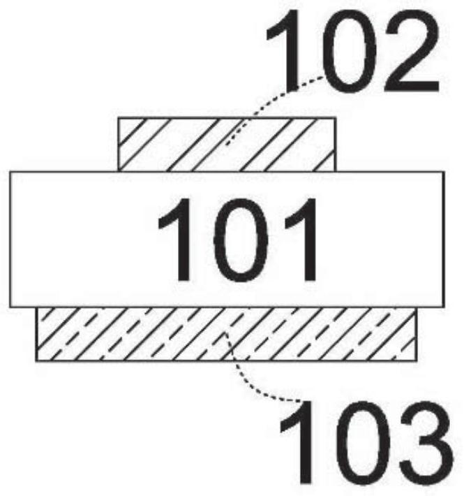
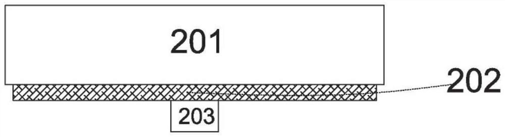
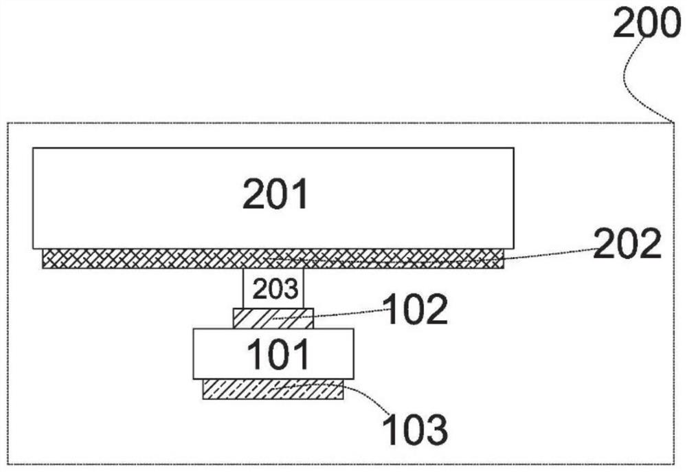
[0100] This embodiment provides a micron-scale device module for fluid assembly and a corresponding manufacturing method, wherein the functions of the micron-scale functional chips included in each micron-scale device are the same.

[0101] see Figure 1a-Figure 1e , Figure 1a-Figure 1e A schematic diagram of the components and the overall structure of a fluid-assembled micron-scale device module provided in Embodiment 1 is shown, wherein Figure 1a It is a schematic cross-sectional structure diagram of a micron-level functional chip, the micron-level functional chip is a vertical structure chip, and the micron-level functional chip has a first electrode 102 and a second electrode 103; Figure 1b is the cross-sectional structure of the intermediary substrate, the intermediary substrate has a conductive layer 202 and a soldering layer 203; Figure 1c Shows the structure of a micron-scale device 200 composed of a micron-scale functional chip and an intermediary substrate; F...

Embodiment 2

[0134] This embodiment provides a micron-level device module for fluid assembly and the corresponding manufacturing process. The functions of the micron-level function chips contained in each micron-level device are different. Typically, there are three micron-level devices with different functions. function chip.

[0135] see Figure 4a , which is a structural schematic diagram of a support substrate in a fluid-assembled micron-scale device module provided in this embodiment. The support substrate is 300, and the main body of the support substrate is provided with a first installation groove 311, a second installation groove 321, The third installation slot 331 is an installation slot with three structures and sizes.

[0136] Figure 4b It is a schematic structural diagram of a fluid-assembled micron-scale device module provided in this embodiment. The fluid-assembled micron-scale device module includes a first micron-scale functional chip 110, a first intermediary substrat...


PUM

PropertyMeasurementUnit
diameteraaaaaaaaaa

Abstract

The invention discloses a fluid assembled micron-sized device module and a manufacturing method thereof. The fluid-assembled micron-sized device module comprises a supporting substrate and a micron-sized device. The micron-sized device comprises a micron-sized functional chip and an intermediate substrate, the micron-sized functional chip comprises an epitaxial structure, a first electrode and a second electrode, the first electrode and the second electrode are arranged on the two sides of the epitaxial structure in a back-to-back mode respectively. The first electrode is electrically connected with the intermediate substrate; when the micron-sized device is combined with the supporting substrate in a fluid assembly mode, the second electrode of the micron-sized device is directly and electrically connected with the circuit wiring layer, and the first electrode of the micron-sized device is electrically connected with the circuit wiring layer through the intermediate substrate. According to the invention, the size of the micron-sized chip is reduced, the cost of the large-scale micron-sized device module is greatly reduced, the micron-sized functional chip and the micron-sized device can be selected through a preselection test, and the yield of the large-scale micron-sized device module is greatly improved.

Description

technical field [0001] The invention particularly relates to a fluid-assembled micron-level device module and a manufacturing method thereof, belonging to the technical field of semiconductors. Background technique [0002] Micro-LED technology is a technology for miniaturizing and arraying light-emitting diode (LED) chips, which refers to the integration of high-density micro-sized LED arrays on one chip. Micro-LED display technology refers to the use of Micro-LED as a light-emitting unit, the production of Micro-LED arrays through mass transfer and / or bonding technology and the integration of them with driving circuits to achieve individual addressing and lighting of Micro-LEDs. Target, so as to achieve monochrome or blue, green, red (RGB) three-color light emission, forming a high-resolution display. Compared with other display technologies, Micro-LED display technology has obvious advantages. First of all, the power consumption of LED is very low in theory, which is abo...

Claims


Application Information

Patent Timeline
Patent Type & Authority Applications(China)
IPC IPC(8): H01L33/62H01L33/36H01L25/075
CPCH01L33/62H01L33/36H01L25/0753H01L2933/0066H01L2933/0016
Inventor 周玉刚贾先韬许朝军张荣
Owner NANJING UNIV
Why Eureka
Try Eureka