Unlock instant, AI-driven research and patent intelligence for your innovation.

Silicon oxide selective dry etch process

A technology of process and etching rate, applied in the direction of electrical components, circuits, semiconductor/solid-state device manufacturing, etc., can solve problems such as residues and pattern collapse

Active Publication Date: 2021-05-11
베이징이타운세미컨덕터테크놀로지컴퍼니리미티드 +1
View PDF5 Cites 0 Cited by
  • Summary
  • Abstract
  • Description
  • Claims
  • Application Information

AI Technical Summary

Problems solved by technology

Finally, as mentioned above, wet etch processes can have issues with surface tension induced pattern collapse and post-etch residue inside high aspect ratio structures

Method used


Image

  • Silicon oxide selective dry etch process
  • Silicon oxide selective dry etch process
  • Silicon oxide selective dry etch process

Examples


Embodiment Construction

[0021] Reference will now be made in detail to implementations, one or more examples of which are illustrated in the accompanying drawings. Each example is provided by way of explanation of implementation, not limitation of the disclosure. In fact, it will be apparent to those skilled in the art that various modifications and changes can be made to the embodiments without departing from the scope or spirit of the present disclosure. For example, features illustrated or described as part of one embodiment can be used with another embodiment to yield still a further embodiment. Accordingly, it is intended that aspects of the present disclosure cover such modifications and variations.

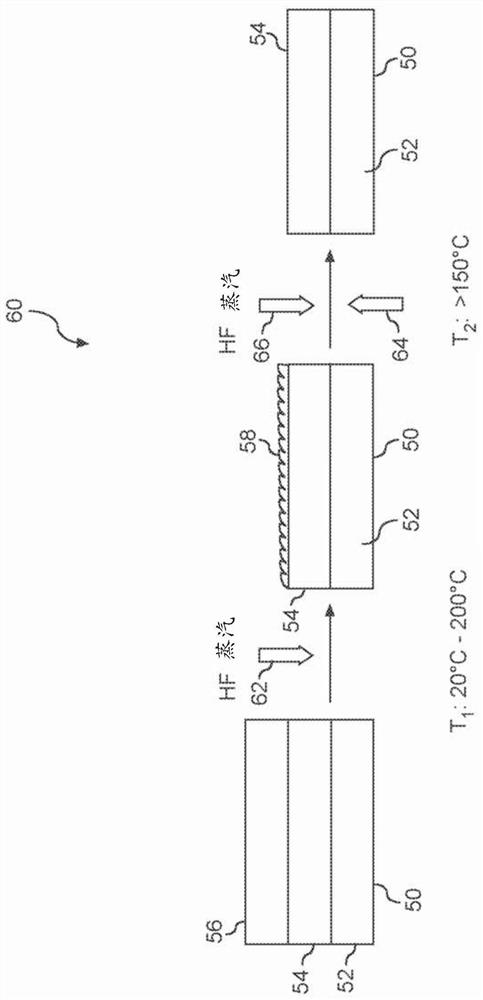
[0022] Example aspects of the present disclosure relate to processing workpieces, such as semiconductor workpieces. For example, example aspects of the present disclosure relate to processes for removing doped silicate glass materials (eg, BSG, PSG, and BPSG) with high selectivity relative to ot...


PUM


Abstract

Systems and methods for processing a workpiece are provided. In one example, a method includes exposing the workpiece to a first gas mixture when the workpiece is at a first temperature to conduct a doped silicate glass etch process. The first gas mixture can include hydrofluoric acid (HF) vapor. The doped silicate glass etch process at least partially removes the doped silicate glass layer at a first etch rate that is greater than a second etch rate associated with removal of the at least one second layer. The method can include heating the workpiece to a second temperature. The second temperature is greater than the first temperature. The method can include exposing the workpiece to a second gas mixture when the workpiece is at a second temperature to remove a residue from the workpiece.

Description

[0001] priority statement [0002] This application claims priority to US Application Serial No. 16 / 557,346, filed August 30, 2019, entitled "Silicon Oxide Selective Dry Etch Process," which is incorporated by reference. technical field [0003] The present disclosure generally relates to the processing of workpieces, such as semiconductor workpieces. Background technique [0004] Processing of semiconductor workpieces can involve depositing, patterning, and removing layers of different materials on a substrate to form multilayer structures. For better patterning contrast in the fabrication of 3D device structures, each layer is approximately planar. Within each layer, a dielectric material such as silicate glass can be used to separate structures and insulate conductive materials. Doped silicate glasses, including borosilicate glass (BSG), phosphosilicate glass (PSG) and borophosphosilicate glass (BPSG), are commonly used as dielectric or insulating layers between conduct...

Claims


Application Information

Patent Timeline
IPC IPC(8): H01L21/311H01L21/67
CPCH01L21/31116H01L21/67253H01L21/0206H01L21/32137
Inventor 张祺吕新亮仲華杨海春
Owner 베이징이타운세미컨덕터테크놀로지컴퍼니리미티드