Semiconductor process equipment

A process equipment, semiconductor technology, applied in semiconductor/solid-state device manufacturing, metal material coating process, vacuum evaporation plating and other directions, can solve problems such as poor film uniformity, achieve high uniformity, improve uniformity, and improve product quality. rate effect

Active Publication Date: 2021-05-14
BEIJING NAURA MICROELECTRONICS EQUIP CO LTD
View PDF9 Cites 0 Cited by
  • Summary
  • Abstract
  • Description
  • Claims
  • Application Information

AI Technical Summary

Problems solved by technology

[0004] When the film growth process is carried out through the existing semiconductor process equipment, the film often has poor uniformity problems, and after the workpiece is taken out of the process chamber and the uniformity problem is found, it is often impossible to remedy

Method used


Image

  • Semiconductor process equipment
  • Semiconductor process equipment
  • Semiconductor process equipment

Examples


Embodiment Construction

[0028] Specific embodiments of the present invention will be described in detail below in conjunction with the accompanying drawings. It should be understood that the specific embodiments described here are only used to illustrate and explain the present invention, and are not intended to limit the present invention.

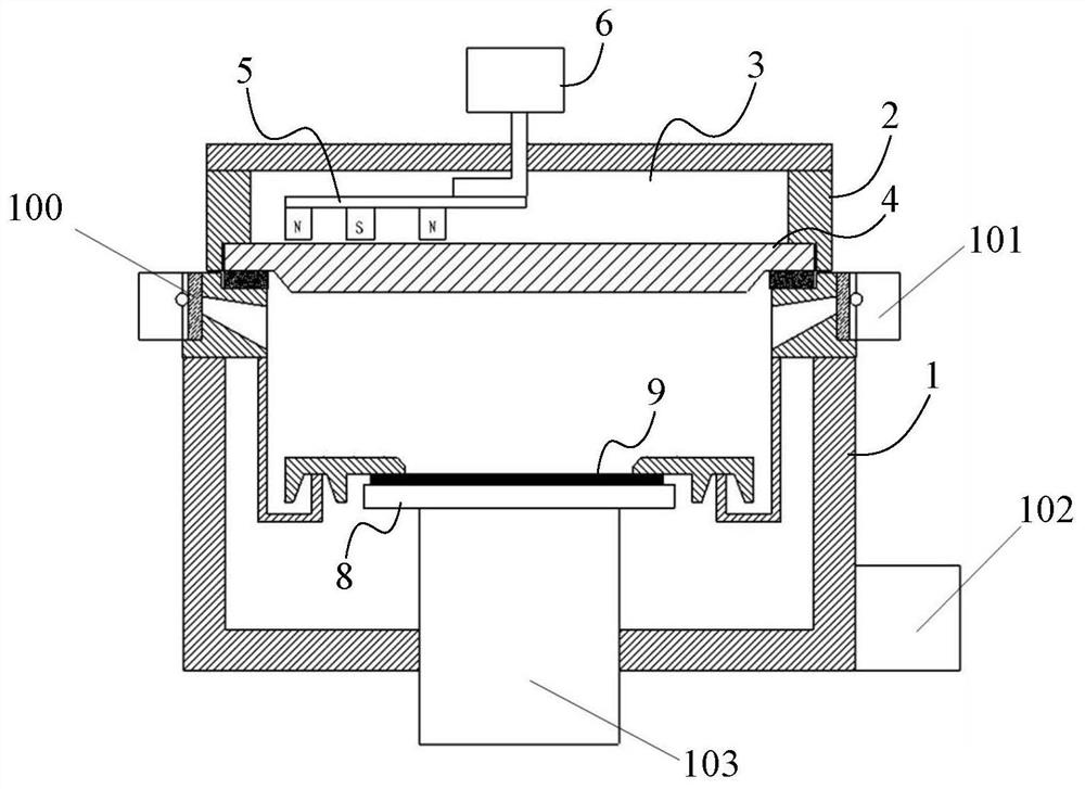
[0029] In order to solve the above technical problems, the present invention provides a semiconductor process equipment, such as figure 1 As shown, the semiconductor process equipment includes a process chamber 1 and a carrier plate 8 arranged in the process chamber 1, the semiconductor process equipment also includes a thickness detection device, a carrier plate lifting device 103 and a control device 102, the thickness detection device is used for Send detection light signals to multiple detection positions of the substrate 9 on the carrier disc 8 and receive reflected light signals of multiple detection positions, and determine the thickness of the substrate ...


PUM


Abstract

The invention provides semiconductor process equipment. The equipment comprises a process chamber, a bearing disc arranged in the process chamber, the equipment further comprises a thickness detection device, a bearing disc lifting device and a control device, the thickness detection device is used for emitting detection light signals to a plurality of detection positions of a substrate on the bearing disc, receiving reflection light signals of the plurality of detection positions and determining the thickness of the substrate at the plurality of detection positions according to the reflection light signals, and the control device is used for determining the thickness uniformity of the substrate according to the thickness of the substrate at the plurality of detection positions, and controlling the bearing disc lifting device to adjust the height of the bearing disc when the uniformity is higher than the preset uniformity. According to the semiconductor process equipment, the uniformity of a film layer on the surface of the substrate can be adjusted in real time in the sputtering process, the product yield is improved, and the production cost is reduced.

Description

technical field [0001] The present invention relates to the field of semiconductor process equipment, in particular to semiconductor process equipment. Background technique [0002] Physical vapor deposition technology (Physical Vapor Deposition, PVD) is widely used in the semiconductor industry. It has the advantages of low process temperature, fast deposition rate, less impurities, environmental protection and no pollution. Magnetron sputtering is the most important one in PVD technology. The basic principle of sputtering coating is to make the argon gas glow discharge under the vacuum condition filled with argon (Ar) gas, at this time, the argon (Ar) atoms are ionized into argon ions (Ar+), under the action of electric field force, argon ions accelerate the bombardment of the cathode target made of plating material, and the target material will be sputtered out and deposited on the surface of the workpiece. Magnetron sputtering can not only deposit metal films such as Au...

Claims


Application Information

Patent Timeline
Patent Type & Authority Applications(China)
IPC IPC(8): C23C14/54C23C14/35H01L21/67
CPCC23C14/547C23C14/35H01L21/67253
Inventor 胡烁鹏
Owner BEIJING NAURA MICROELECTRONICS EQUIP CO LTD
Why Eureka
Try Eureka