Base with coil, periscopic voice coil motor and manufacturing method thereof
A coil and base technology, which is applied in the manufacture of motor generators, the shape/style/structure of winding insulation, and the connection with control/drive circuits, etc., can solve the problems of high overall cost, affecting the coil current, and low efficiency. Achieve the effects of compact and miniaturized structure, mass production, and reduced assembly costs
- Summary
- Abstract
- Description
- Claims
- Application Information
AI Technical Summary
Problems solved by technology
Method used
Image

Examples
Embodiment Construction
[0047] In the description of the present invention, it should be noted that the orientation or positional relationship indicated by the terms "upper", "lower", "inner", "outer" and the like are based on the orientation or positional relationship shown in the accompanying drawings, and are only for It is convenient to describe the present invention and simplify the description, but does not indicate or imply that the device or component referred to must have a specific orientation, be constructed and operate in a specific orientation, and thus should not be construed as limiting the present invention.
[0048] In the description of the present invention, it should be noted that, unless otherwise clearly specified and limited, the term "connection" should be understood in a broad sense, and those of ordinary skill in the art can understand the above terms in the present invention in specific circumstances. specific meaning.
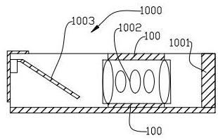
[0049] The periscope voice coil motor in the prior ar...
PUM
 Abstract
Description
Claims
Application Information
 - R&D
- Intellectual Property
- Life Sciences
- Materials
- Tech Scout
- Unparalleled Data Quality
- Higher Quality Content
- 60% Fewer Hallucinations
Browse by: Latest US Patents, China's latest patents, Technical Efficacy Thesaurus, Application Domain, Technology Topic, Popular Technical Reports.
© 2025 PatSnap. All rights reserved.Legal|Privacy policy|Modern Slavery Act Transparency Statement|Sitemap|About US| Contact US: help@patsnap.com