Eureka AIR delivers breakthrough ideas for toughest innovation challenges, trusted by R&D personnel around the world.

Full-automatic wafer appearance inspection system

A visual inspection, fully automatic technology, applied in the direction of conveyor objects, electrical components, semiconductor/solid-state device manufacturing, etc., can solve the problem that the inspection system cannot meet the inspection requirements

Pending Publication Date: 2021-05-18
无锡奇众电子科技有限公司
View PDF0 Cites 4 Cited by
  • Summary
  • Abstract
  • Description
  • Claims
  • Application Information

AI Technical Summary

Problems solved by technology

Existing detection systems cannot meet the above detection requirements

Method used


Image

  • Full-automatic wafer appearance inspection system
  • Full-automatic wafer appearance inspection system
  • Full-automatic wafer appearance inspection system

Examples


Embodiment Construction

[0021] Specific embodiments of the present invention will be described in detail below in conjunction with the accompanying drawings.

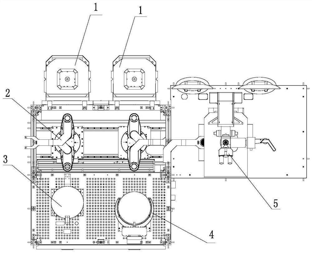
[0022] like figure 1 As shown, the fully automatic wafer appearance inspection system of the present invention includes a wafer box unpacking carrier 1, a wafer pick-and-place manipulator 2, a wafer position calibration mechanism 3, a wafer turning mechanism 4, and a microscope detection mechanism; The wafer box unpacking carrier is used to open the wafer transfer box, the wafer pick-and-place manipulator is used to carry the wafer, and the wafer position calibration mechanism is used to determine the position of the center of the wafer and rotate it to An angle is specified; the wafer turning mechanism is used to turn over the wafer so as to inspect the back side thereof, and the microscope inspection mechanism checks the wafer surface.

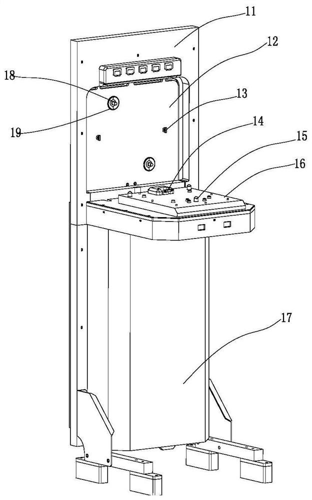
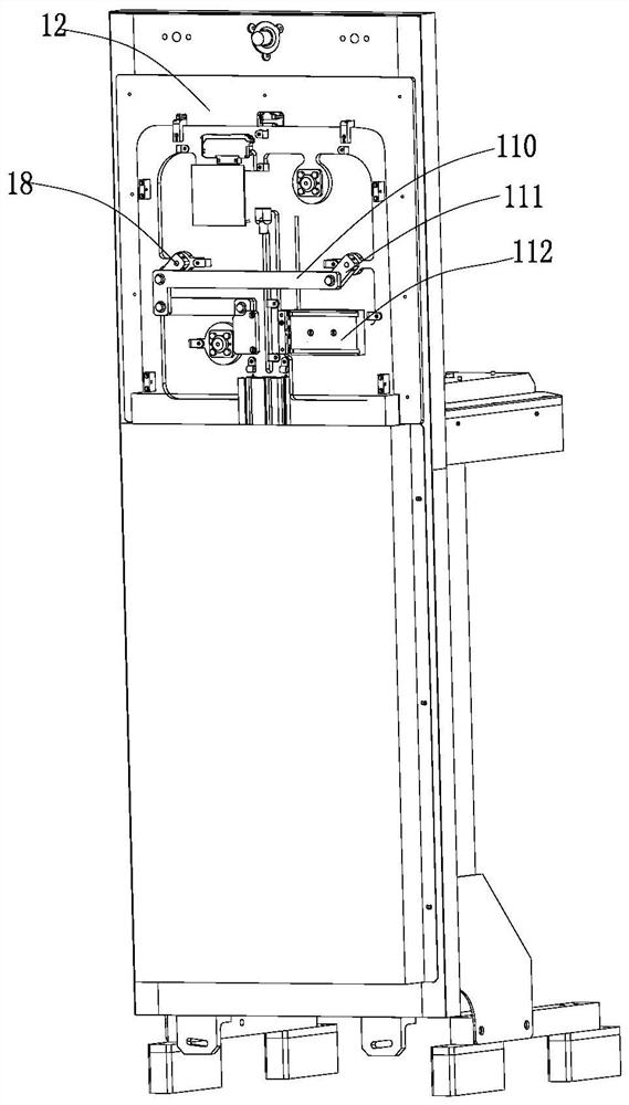
[0023] Wherein the specific structure of the wafer box unpacking carrier 1 is as follows: figure 2 and...


PUM


Abstract

The present invention relates to a full-automatic wafer appearance inspection system which comprises a wafer box opening carrier, a wafer taking and placing manipulator, a wafer position calibration mechanism, a wafer turnover mechanism and a microscope detection mechanism, the wafer box opening carrier is used for opening a wafer conveying box, the wafer taking and placing manipulator is used for carrying wafers, and the wafer position calibration mechanism is used for determining the circle center position of the wafer and rotating the wafer to a specified angle; and the wafer turnover mechanism is used for turnovering a wafer so as to inspect the back surface of the wafer, and the microscope detection mechanism inspects the surface of the wafer. The wafer can be automatically transmitted to the microscope for observation, so that damage caused by manual carrying is avoided; the surface and the back surface of the wafer can be visually inspected; and linear motion is adopted in the transmission process, and the wafers are prevented from being thrown out. The system is suitable for being used in semiconductor factories and wafer test factories.

Description

technical field [0001] The invention relates to the technical field of electronic detection, in particular to a wafer appearance inspection system. Background technique [0002] Wafer refers to the silicon wafer used to make silicon semiconductor circuits, and its raw material is silicon. High-purity polycrystalline silicon is dissolved and mixed with silicon crystal seeds, and then slowly pulled out to form cylindrical single crystal silicon. After the silicon ingot is ground, polished, and sliced, it forms a silicon wafer, that is, a wafer. At present, domestic wafer production lines are mainly 8-inch and 12-inch. [0003] Manufacturers often have to inspect their quality during delivery or receipt. Wafer cassettes are generally stored in FOUPs, which need to be taken out one by one for inspection. During the wafer turnover process, the position and direction of the center of the wafer will be shifted by a small angle. In addition, the back of the cassette needs to be i...

Claims


Application Information

Patent Timeline
Patent Type & Authority Applications(China)
IPC IPC(8): H01L21/66H01L21/67H01L21/677H01L21/68
CPCH01L22/12H01L21/681H01L21/67265H01L21/67748H01L21/67742
Inventor 肖宇易涛岳湘罗嘉涵
Owner 无锡奇众电子科技有限公司
Why Eureka
Eureka Blog
Learn More