A kind of dimer small molecule electron donor material and its preparation method
A technology of electron donor materials and electron acceptor materials, applied in the field of solar cells, can solve the problems of low photoelectric conversion efficiency of solar cells, achieve huge application potential and value, improve photoelectric conversion efficiency, and good solubility
- Summary
- Abstract
- Description
- Claims
- Application Information
AI Technical Summary
Problems solved by technology
Method used
Image
Examples
Embodiment 1
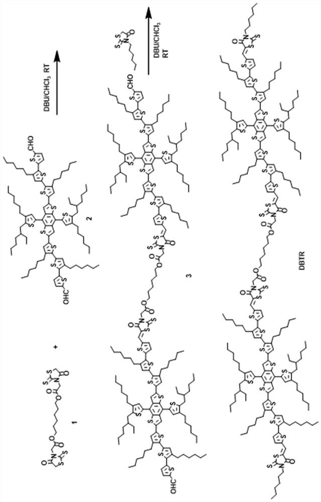
[0061] figure 1 Shown is a schematic diagram of the synthesis process of the dimer small molecule electron donor material in this example.
[0062] Such as figure 1 As shown, the preparation process of the dimer small molecule electron donor material is as follows:
[0063] 1. Synthesis of Compound 3
[0064] Compound 1 (0.1000g, 0.0613mmol purchased from Ruixun) and compound 2 (0.0057g, 0.0122mmol purchased from Gia) were dissolved in 10 ml of chloroform, and then DBU (1,8-diazabicycloundec- 7-ene) 0.1 ml. The reaction was stirred at room temperature for 0.5 hours. Then the solvent is removed under reduced pressure, separated by silica gel column chromatography, the eluent is chloroform / petroleum ether (by volume, chloroform:petroleum ether=3:1), the product compound 3 is a red solid (0.0450g, the yield is 1% of the theoretical yield) 55.48%).
[0065] Characterization data of compound 3: 1 H NMR (600MHz, Chloroform-d) δ9.86(s,2H),7.84(s,2H),7.67(d,J=4.0Hz,2H),7.61(s...
Embodiment 2
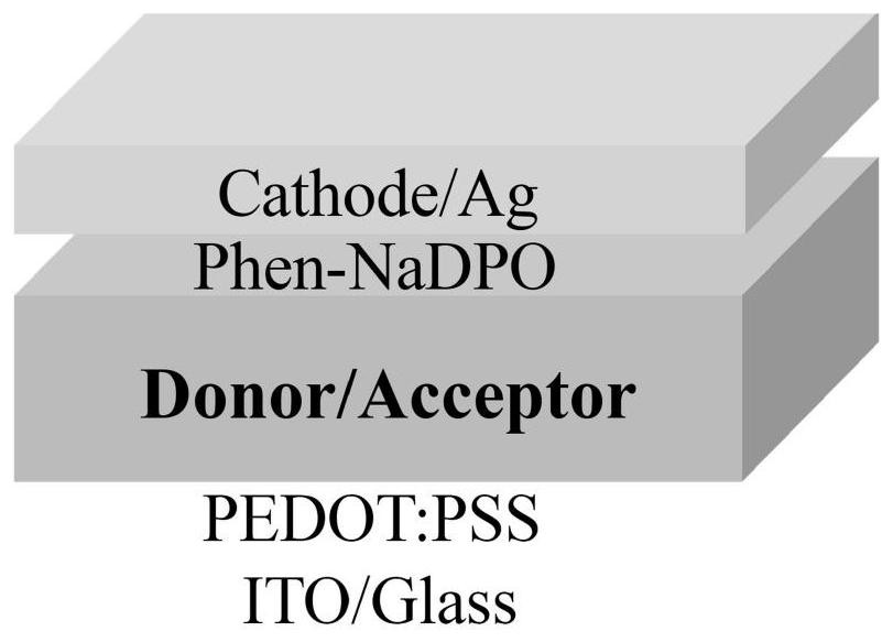
[0071] Adopt embodiment 1 to make dimer small molecule electron donor material (i.e. figure 1 Shown DBTR) prepares a kind of whole small molecule organic solar cell, and concrete preparation process is as follows:
[0072] A kind of all-small-molecule organic solar cell is prepared by using BTR purchased on the market as the electron donor material, and the specific preparation process is as follows:
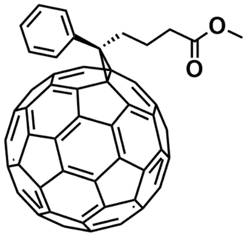
[0073] The substrate composed of transparent glass and transparent conductive electrode ITO was ultrasonically cleaned with cleaning solution, deionized water, acetone and isopropanol, and dried with nitrogen after cleaning; the substrate was placed in an ozone cleaner for 15 minutes , Spin-coat the hole transport layer material PEDOT:PSS in air (4000rpm, 20s, film thickness 30nm), then perform thermal annealing in air (120°C, 10min), and then transfer the sample into a glove box filled with nitrogen , the active layer (DBTR:PC 71 BM=1:1, 40mg / ml, active layer film thickness:...
PUM
| Property | Measurement | Unit |
|---|---|---|
| thickness | aaaaa | aaaaa |
| thickness | aaaaa | aaaaa |
| thickness | aaaaa | aaaaa |
Abstract
Description
Claims
Application Information


